HLv2 Beta3 PA Mode test result


Steve Haynal

in3otd
thanks for the detailed measurements; at a first glance the PA seems to work as expected.
Regarding T3, I remember checking the transformer temperature when transmitting at 1.8 MHz and 30 MHz for 1 minute or so and while it was certainly warm it didn't seem particularly hot. At which frequency and power level did you test the transformer temperature?
Takashi K
The test frequency is 14.025MHz and PA output power is around 5W at full power setting (PowerSDR Drive Level 100).
Takashi K
> (no direct connection) from TX to RX. I think there is enough of that
> happening with the HL2 too.
Steve Haynal
Takashi K
Steve Haynal
Takashi K
Steve Haynal
Takashi K
Steve Haynal
Takashi K
in3otd
Hello Taka,
the spectra in the pdf file you enclosed above show a
carrier at around -10 dBm on the spectrum analyzer (e.g in the 20 m
band), which taking into account the 20 dB + 30 dB of attenuation you
had would mean an output of 40 dBm so more than you reported later - not
sure which numbers are the right ones, hi.
The inductance values you
measured for the transformer look reasonable, at low frequency that
core gives about 10 uH/turn^2, with nominally a 30 % tolerance.
I did not yet test the PA here, for the moment I have some measurements on the driver - modified with R55 at 120 ohm:
here is the output power at the fundamental over frequency, for different drive levels in Quisk:

Flatness is a bit worse than the H-Lv2b2 here, maybe due to the different transformer used - even if also the current one should have enough bandwidth.
Here are the fundamental and harmonics over frequency at max output:

Out of curiosity, I checked also the driver output after enabling/disabling the PA path and also my H-Lv2b3 did have very little or no output at the beginning, which then increased over time - applying 5.6 kohm resistors to ground to U10 pin5 and U11 pin 5 as suggested solved this issue. A bit puzzling that the H-Lv2b2 here works fine without the additional resistors.
73 de Claudio, IN3OTD / DK1CG
Takashi K
> dBm on the spectrum analyzer (e.g in the 20 m band), which taking into
> account the 20 dB + 30 dB of attenuation you had would mean an output of 40
> dBm so more than you reported later
So they are not suitable to measure absolute power value.
The voltage at dummy is measured by Scope.
DVM and Scope are commercial products, but cheap.
So, I don't know which is right exactly.
> low frequency that core gives about 10 uH/turn^2, with nominally a 30 %
> tolerance.
in3otd
Hello,
here are some measurements on the H-Lv2b3 TX IMD; the results look quite good, similar to what measured previously on the H-Lv2b2, taking into account that the drive level to the PA is now lower and its supply is also lower.

The usual ripples in the IMD due to the DC/DC converter behavior can clearly be seen there but should not cause any issue.
I saw once that the TX output was a few dB lower than expected, not sure if because I did not stop the measurement script properly and left the H-L in some "undefined state" but after turning the board off and on again everything was fine. Not sure if this is similar to what Taka saw.
73 de Claudio, IN3OTD / DK1CG
Steve Haynal
Takashi K
in3otd
here is the H-Lv2b3 PA output vs frequency for the various TxPGA settings:

and here are the harmonics at maximum output (TxPGA 15):

the output is not as flat as in the H-Lv2b2, likely die to the driver, as said in the other post.
Harmonics are relatively low, maybe a little better than seen previously.
73 de Claudio, IN3OTD / DK1CG
in3otd
I've checked again the T3 transformer temperature: at 14.2 MHz and full PA output (about 8.3 W) after about 2 minutes of transmission it actually gets quite warm: I did not measure it yet but it feels to the touch at least as warm as the AD9866, so maybe around 45 C.
73 de Claudio, IN3OTD / DK1CG
Takashi K
vertical). like this,

Alan Hopper
73 Alan M0NNB
Steve Haynal
Takashi K
I was using UEW wire but shorted with core.
in3otd
glad to know that your PA is working fine now - you actually get a little more power than I here now, hi.
It's true that the core has a very low resistivity and a wire touching the core could cause issues. Using FEP wire will be the best solution (and it's always silver plated, AFAIK), maybe we could ask the manufacturer to include a short length of wire with the H-L.
Out of curiosity, is the new transformer getting hot as the old one during your tests?
73 de Claudio, IN3OTD / DK1CG
Takashi K

Graeme Jury
73, Graeme zl2apv
Takashi K
Steve Haynal
Steve Haynal
in3otd
Hello,
I was referring to the post just above
where the driver output is plotted vs. frequency; in the H-Lv2b3 the
driver output peaks at about 17 dBm at 14 MHz and goes down to 15 dBm at
30 MHz. In the previously measured drivers the drop at high frequency
was quite less; a summary of the measured PA drivers outputs for the various versions is in the graph below

note that I have added 3.57 dB to the H-Lv2b3 driver output to account for the lower gain due to the R55 change. I'm somewhat surprised by the close agreement at low frequency, hi. But at the upper end the H-Lv2b3 driver output is about 1 dB less than previously seen, starting from about 25 MHz.
I tried restoring R55 to the old 75 ohm value but the output vs. frequency curve shape did not change at all, just shifted up as expected. I've also changed the MABAES0060 transformer with the BN43-2402 one I've used previously but again the output stayed the same - so this confirms that this transformer is working well. At this point I do not know why the H-Lv2b3 driver output drops above 25 MHz, it could be that the components in the filter ahead of the driver have too much tolerance or a value is wrong but I did not yet try to desolder and measure them.
Alan Hopper
Alan Hopper
Steve Haynal
Alan Hopper
Alan Hopper
in3otd
can you measure the output power vs frequency and compare with the graphs I posted previously, to check if the filter is working fine or some components there is wrong? The driver output will saturate at about 23 dBm and the distortion will increase rapidly near that level.
73 de Claudio, IN3OTD / DK1CG
Takashi K
Alan Hopper
Steve Haynal
Alan Hopper
Alan Hopper
Takashi K
Alan Hopper
Steve Haynal
Alan Hopper
Steve Haynal
Steve Haynal
Takashi K
in3otd
I replaced just R56 and R59 for the moment, I still get the same power output over frequency. Measuring the resistors with a VNA, the ones originally mounted and the Yageo used as replacements look practically identical - with just a parallel parasitic capacitance around 0.5 pF.
73 de Claudio, IN3OTD / DK1CG
Steve Haynal
Steve Haynal
Steve Haynal
Steve Haynal
Takashi K
Alan Hopper
On Saturday, September 9, 2017 at 7:16:24 AM UTC+1, Steve Haynal wrote:
Hi Alan,
Steve Haynal
Steve Haynal
in3otd
Hello,
today I removed all the PA driver input filter components and
measured them on a VNA; from what I could see they looked ok and quite
similar to the ones I used for the H-Lv2b2 - except maybe the
capacitors, for which it was difficult to precisely measure the
losses/Q.
Since I suspected that some/all of the capacitors might not
have a very high Q, I changed them all (C49, C50, C51 and C52) with the
spares I had from the previous build. Besides R56 and R59, which were changed previously with no measurable effect, I didn't change anything else.
This made quite a difference on the PA output level flatness:

and here is a comparison with the H-Lv2b2 output (here have added 3.57 dB to the H-Lv2b3 driver output to account for the lower gain)

so now the PA driver output flatness is practically the same as on the H-Lv2b2.
Since I changed all the caps together I do not know if there were just 1 or 2 caps which caused the high-frequency level drop. If you would like to experiment changing the driver filter caps on your H-Lv2b3, you may use the RX at minimum gain and an additional 30 dB or 40 dB of attenuation to check the PA driver level; the absolute values may be off due to the RX response being not completely flat but you should be able to compare the effect on the PA driver output when changing some component.
I'll later check how the PA output flatness looks like after these changes.
73 de Claudio, IN3OTD / DK1CG
Steve Haynal
| 150pF 0805 NP0>=50V<=5% | CC0805JRNPO0BN151 | Y | C50 | 805 | 2 | 1 | http://www.octopart.com/search?q=CC0805JRNPO0BN151 | ||||||
| 160pF 0805NP0>=50V<=5% | GRM2165C2A161JA01D | Y | C51 | 805 | 2 | 1 | http://www.octopart.com/search?q=GRM2165C2A161JA01D | ||||||
Steve Haynal
in3otd
Hello Steve,
C49 : 72.5 pF, -3.4 % w.r.t. the 75 pF nominal
C50 : 153 pF, +2 % w.r.t. the 150 pF nominal
C51 : 143 pF, -10,6 % w.r.t. the 160 pF nominal
C52 : 99.5 pF, -0.5 % w.r.t. the 100 pF nominal
so the measured C51 value is way out of tolerance.
The PA driver simulations done some time ago never matched exactly the measurements but out of curiosity I re-simulated the driver filter response with the nominal and the actual C51 value.
This is the response with the filter nominal values

the simulation results have less ripple and drop at the high end but the peaks and valleys are more or less at the right position.
Here is a comparison between a simulation with C51 set to 143 pF and the H-Lv2b3 driver output before reworking the filter:

again, the response is a bit different but the general trend is the same.
So I'll say that very likely the issue, at least on my board, came from the wrong C51 value and is not related to the capacitors quality/losses.
Maybe they mistakenly installed a 140 pF capacitor on all the boards for C51, instead of 160 pF or even mixed up more values in the filter area in the other boards.
I wonder if it makes sense to use 150 pF in parallel with 10 pF, as these values are already in the BOM to avoid the non-standard 160 pF.
73 de Claudio, IN3OTD / DK1CG
Alan Hopper
Steve Haynal
Alan Hopper
Steve Haynal
Alan Hopper
Hi Alan,
Alan Hopper
Steve Haynal
Alan Hopper
Steve Haynal
in3otd
I remember measuring on the H-Lv2b2 and there the supply was quite clean - actually a bit cleaner at high current than at low current, due to the DC/DC pulse skipping, IIRC.
Alan, can you try to simply load the DC/DC with a resistor, there should be no need to remove T3, if you set the bias to zero; the current monitor is quite precise down to 10 mA or less, once you remove the opamp in the path, so you can also use that to double check the load the DC/DC is seeing.
73 de Claudio, IN3OTD / DK1CG
Takashi K
Have you checked the resistance of R123 using Ohm meter?
Was it 0.04 ohms or lower ?
in3otd
I've measured the PA output and the Vpa level on my H-Lv2b3 and at a first glance they seem fine:

Vpa above was measured on the vias near T3 and B100; with no load it measures 8.0 V.
The measured ripple depends a bit on the time scale used; here at 1.8 MHz and full power, still near B100, I see this

but at a slower time base also this

the reading depends anyway on the probe position, I think there is some RF noise picked up there.
Measuring near the DC/DC converter, on DB14, I sometimes see some jumps in the voltage, at low power and at full power, does not make much difference:

but a similar behavior I see also on the other DC/DC converters, so I guess it might be a "feature" of the converter.
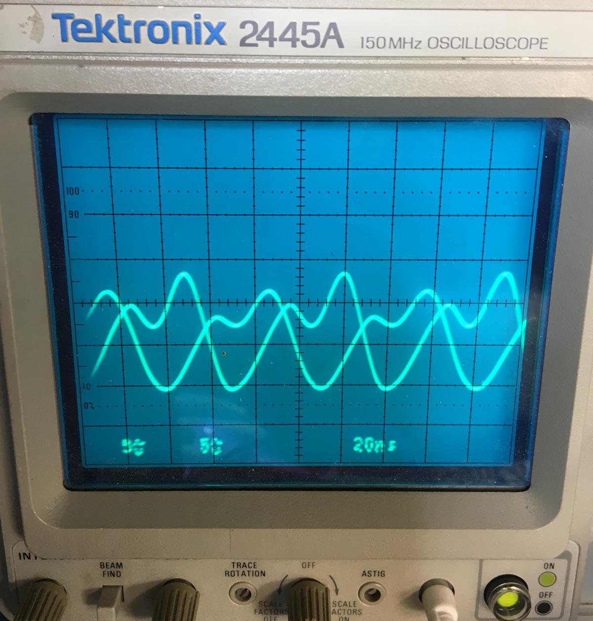
Finally, the regulation seen with a two-tone test, still at full power at 1.8 MHz on DB14, seems not too bad

73 de Claudio, IN3OTD / DK1CG
in3otd
Measuring near the DC/DC converter, on DB14, I sometimes see some jumps in the voltage, at low power and at full power, does not make much difference:
I've checked on the H-Lv2b2, I see the same voltage jumps on the 1.2 V and 3.3 V outputs only just after power up with a "cold" board, they disappear after a few seconds. Powering down and up again I no longer see them.
On the VPA supply they are always present instead, I don't remembering having noticed that before.
I'm wondering whether the converter control loop is somewhat unstable and changing the 4.7 nF cap on the voltage divider could help.
Alan Hopper
Steve Haynal


Steve Haynal
Alan Hopper
in3otd
I also used a spring ground clip for the measurements, place like this

I've remeasured the ripple/noise there to double check and I get the same results, maybe even a little less.
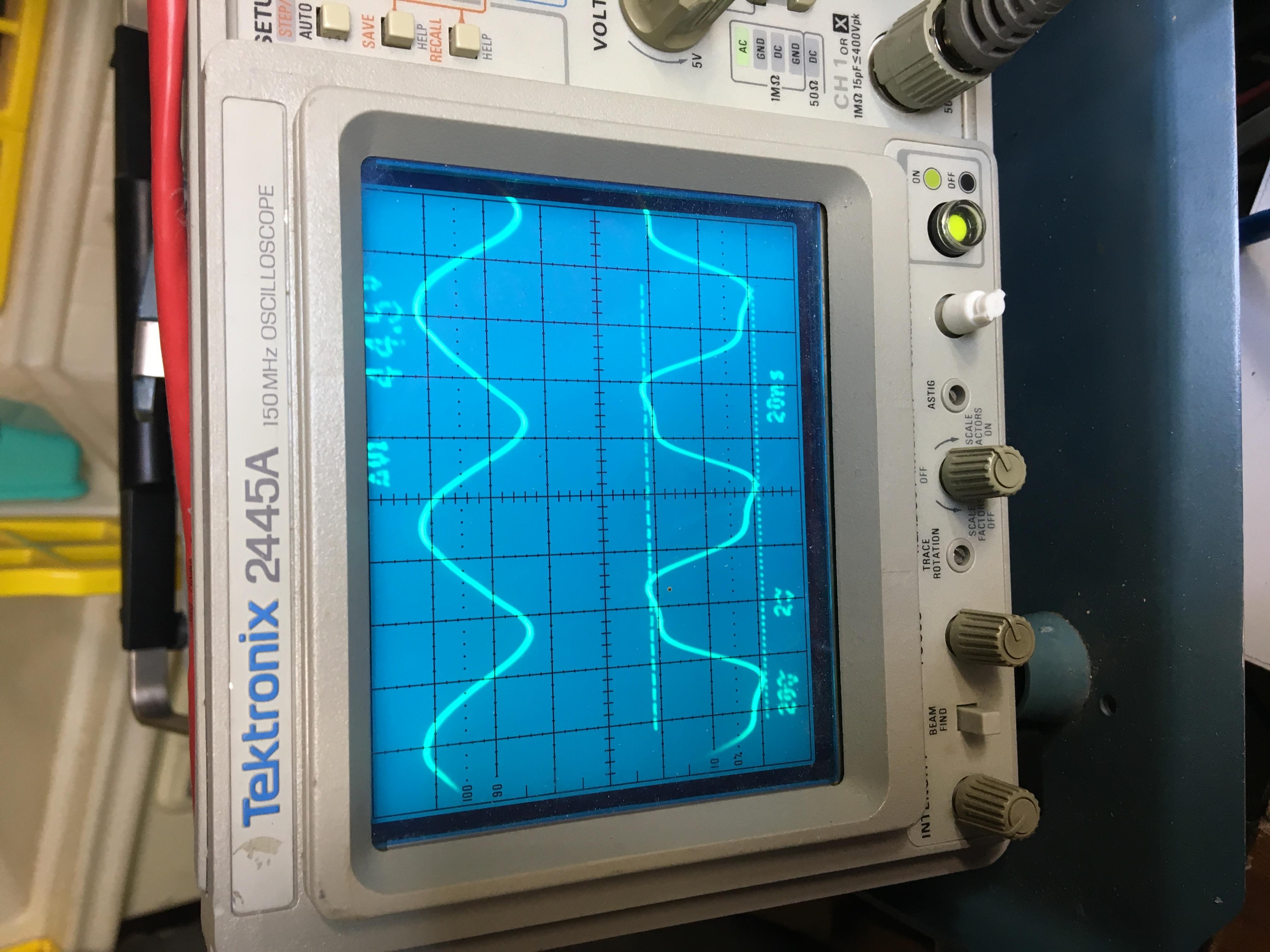
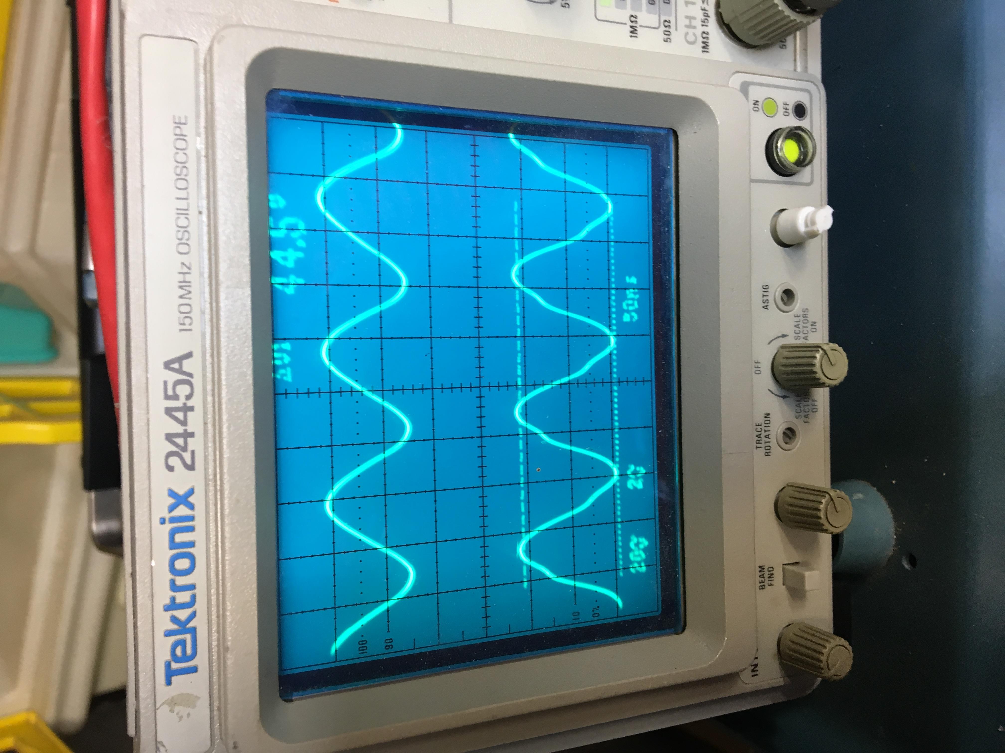
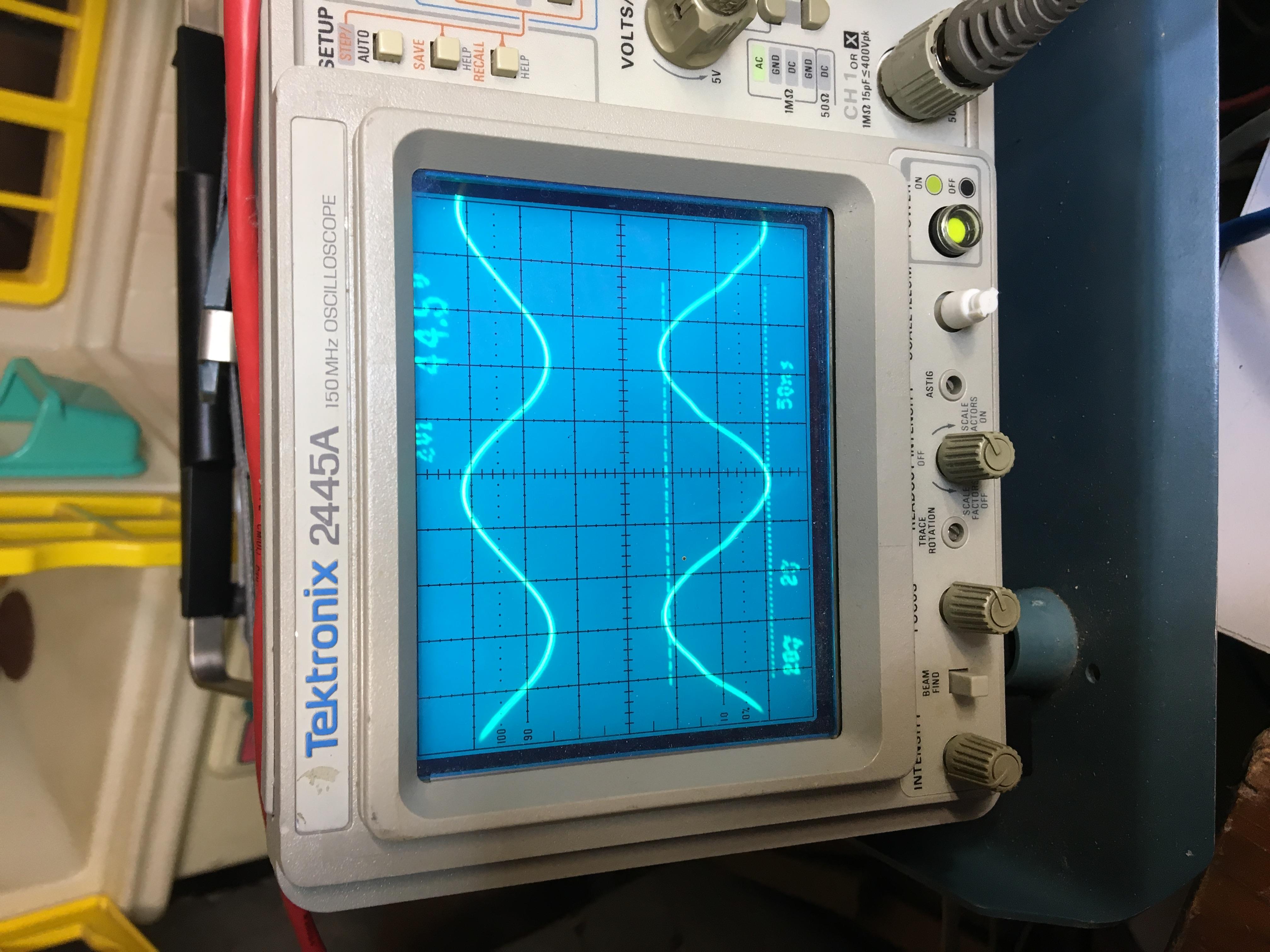
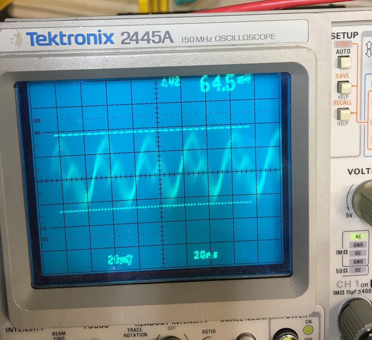
The measurements above were done at 1.8 MHz; as you saw, at 3.8 MHz the ripple on the Vpa supply increases and with the TX at this frequency, I see about 200 mV peak-to-peak near B100:

Note that 3.8 MHz is more or less where the 2nd harmonic has a maximum also(see bottom graph here); it was roughly the same also in the H-Lv2b2.
The waveform on the LDMOS drains looks slightly flattened at the top, so this may be similar to what you see also:

Alan Hopper
in3otd
I'm not sure but I think the ripple peak at 3.8 MHz could be due to the power supply decoupling network having an impedance peak there, due to interactions of the bypass caps with the inductive output impedance of the DC/DC or the inductance of the supply trace. If this is the case moving one of the 22 uF filtering caps near T3 could help moving the peak and reducing its magnitude.
73 de Claudio, IN3OTD / DK1CG
