Remaining PCB issues

946 views
Skip to first unread message

James Ahlstrom

unread,
Mar 24, 2017, 5:30:02 PM3/24/17
to Hermes-Lite
Hello Group,

There is an "Issues" page on the Hermes-Lite2 Git site, but it doesn't attract much traffic.  I thought it might be useful to hash out all remaining HL2 PCB issues here, and then I will transfer the decision to "Issues" and people can start finishing up the PCB.  Please let me know when changes are approved (mostly by Steve) so I know I can change "Issues".  If something has already been decided that is still listed below, please tell me.

1. I suggest we add a 10 uF capacitor to the input of Q1 to provide some protection from static electricity.  This MOSFET is vulnerable to static damage when plugging in power.

2.  The pins 1 and 12 of K2 are reversed.

Now for something more interesting.

3.  Will we still support TO-220 finals?  Things are simpler if we don't.

4.  The digital bias is not finished even though it has its own thread "HL2 Digital Bias Problem".  If we support only AFT05 finals, we just need a resistor from U15 P0A and P1A to ground.  U14 stays at 3.3 volts.  For TO-220 devices, we will need a solution from the thread.  Probably U14 remains so we can switch bias to zero.  Or we can add a separate Enable to U12, eliminate U14 and power bias from U12.  Should we change from 10k to 5k digital pots to lower the source impedance?

5.  There was a proposal to use U12 (opamp driver supply) and connect it to the 12 volt input.  But the U12 Enable is in parallel with the 9 volts PA supply Enable, so turning on the driver (for VNA operation) will turn on the PA supply even though the PA supply does nothing.  I am worried that the PA supply with no load will generate sharp narrow switching regulator spikes and thus noise.  Can we eliminate the Enable for U12?  It draws little current when not producing output.  Or we could add a separate Enable for U12 (see 4 above).  Or we could leave U12 unused and use the PA supply as on the current board.

6.  How do we measure the current in the finals so we can set bias?  I am using a 0.1 ohm resistor.  Do we want to use an ADC channel to measure the current?  Is it worth adding to the protocol to send the data to the PC?

There are more issues to add to this thread, but I would suggest we knock off some of these first.

Jim
N2ADR

John Williams

unread,
Mar 24, 2017, 8:29:55 PM3/24/17
to herme...@googlegroups.com

I agree with Steve on the ease of assembly of the SMD FETs, drop the Mitsubishi devices. They are hard to source and expensive. I was not a fan of the SMD devices but the current data seems to point to stable operation.

John

--
You received this message because you are subscribed to the Google Groups "Hermes-Lite" group.
To unsubscribe from this group and stop receiving emails from it, send an email to hermes-lite...@googlegroups.com.
For more options, visit https://groups.google.com/d/optout.

Graeme Jury

unread,
Mar 24, 2017, 8:50:02 PM3/24/17
to Hermes-Lite
Re item 6. a ZXCT1021 as available from Digikey, connected to an AD input would be a cheap and easy solution.

BTW I have been convinced to go with the AFT05's and see no point in accommodating TO-220 options now. You guys certainly made a good case :-)

Graeme zl2apv

Steve Haynal

unread,
Mar 24, 2017, 10:28:42 PM3/24/17
to Hermes-Lite
Hi Jim and Group,

Yes, please add any issues, even if you are not sure if it is an issue, to the github issues page. This is where I keep track of things that need to be done for the next revision. To minimize problems with miscommunication and file synchronization, I will make all the PCB changes myself, hopefully in the next few weeks.

If someone is itching for a project, KiCAD templates for 5cmx10cm and 10cmx10cm filter boards would be good. I've wanted to do this but have been holding off until the slow ADC has been tested as the position of that IO may change slightly. But, I think all IO is pretty close if someone wants to start.

Regarding Jim's list,

1. Okay. Please file a github issue so I don't forget this.

2. The two pins will be swapped in the next revision.

3. Yes, I still want to support TO-220 devices although they will not be a default build.

We disagree about simplicity. Much of modern engineering is complex to provide a user a simpler and more desirable experience. My smart phone is complex. The automatic tire pressure readings on my car are complex. A modern CPU is complex. Even SDR is more complex than a crystal radio. We go with this extra complexity for a more convenient and desirable user experience. The flexibility I want in the HL2 is for this same purpose. The footprints and NRE have been spent and it is more work to take them off of the PCB.

4. The digital bias is a work in progress. It will be finished for a next revision. Please see this post for the current plan. This should support bias voltages >3.3V as well as finer resolution. I plan to replace the current 3.3V regulator with a mosfet so that the bias voltage can be switched independently. We can go with 5K if shown better.

5. Have you measure the noise your are worried about?

6. This has been discussed. Please see this post: https://groups.google.com/d/msg/hermes-lite/HyXx6w6JBKY/fgVM7t-YBgAJ


73,

Steve
KF7O

Steve Haynal

unread,
Mar 25, 2017, 2:46:30 AM3/25/17
to Hermes-Lite
Regarding the protocol for the slow analog values, we will use the existing AIN1-AIN6 return mechanism. We use this for FWD/REV power on John's board already. The protocol wiki page at  
https://github.com/softerhardware/Hermes-Lite2/wiki/Protocol already specifies which channels to use for what.

73,

Steve
KF7O

James Ahlstrom

unread,
Mar 25, 2017, 9:06:42 AM3/25/17
to Hermes-Lite
Hello Steve,


On Friday, March 24, 2017 at 10:28:42 PM UTC-4, Steve Haynal wrote:
5. Have you measure the noise your are worried about?

No, it is a theoretical concern with switching regulators.  I have mostly been testing on 40 meters, and I see no noise at all.  But here is a suggestion.

5a. Keep the current design as is.

5b. Keep the current design, but add a jumper so that U12 can optionally be powered from the 12 volt supply.  If it is difficult to route 12 volts, this can be a through-hole pad and an air wire.  This is to enable a different future use of the PA supply if it is not used for the PA.  I am not necessarily recommending this, but it is a thought.

Some thoughts:  I am happy not using U12.  It was originally included for voltage protection.  I don't see any problem using Vpa (8 or 9 volts) for U12.  Vpa should always be enough supply voltage.  U12 is rated to produce 2.7 Vpp at a 5 volt supply, and the AFT05s need 2.3 Vpp.  Switching noise should not be a problem since U12 is an opamp with good supply rejection.  And using Vpa for U12 provides the switching regulator with a small load.

Jim
N2ADR

James Ahlstrom

unread,
Mar 25, 2017, 2:00:59 PM3/25/17
to Hermes-Lite
Hello Steve,

On Friday, March 24, 2017 at 10:28:42 PM UTC-4, Steve Haynal wrote:
4. The digital bias is a work in progress. It will be finished for a next revision. Please see this post for the current plan. This should support bias voltages >3.3V as well as finer resolution.

 I see from Claudio's post that we can change to a rheostat part for U15, and these may (or may not) be cheaper or more available in China.  I would still prefer a 5k part if available because high impedance at gates makes me nervous.  But I would suggest keeping the regulator U14 because it is cheap and currently on the board.  It provides regulation from supply voltage sags during transmit when using TO-220 devices.  We need this because the power supply is external and of unknown quality and voltage.  MOSFET amps generally have a regulator here.

4a.  We keep U14 and U15 mostly the same, but add two resistors as per Claudio's post.  The voltage of U14 is 5 volts for the AFT05s and the resistor values for that voltage and a 5k part were provided by Claudio.  If someone wants to use TO-220 finals, they will have to replace U14 with the 10 volt version, and change the resistor values.  This should be OK because Vpa will be 12 volts or higher.  Again, resistor values were provided by Claudio.

4b.  We remove U14 and use Vpa directly and add an RC filter for switching hash.  Bias on/off is provided by adding a MOSFET.  If TO-220 devices are used, Vpa is 12 or 13.6 volts, and we just change resistor values.  There is no protection from supply voltage variations when using TO-220 parts.

4c.  There is currently no way to run the Vpa 9 volt switching supply at the same time as using the external 12 volt input for Vpa.  But if we add one, we could use the regulated 9 volt Vpa for both TO-220 bias and for AFT05 bias.  We still need the MOSFET switch.

Jim
N2ADR

James Ahlstrom

unread,
Mar 25, 2017, 2:31:46 PM3/25/17
to Hermes-Lite
Hello Group,

Regarding option 5, I mixed up some U12 references on my last post.  I should have said:

Some thoughts:  I am happy to use Vpa instead of the voltage regulator U12 to power the driver U9 when using AFT05 devices.  U12 was originally included for voltage protection.  I don't see any problem using Vpa (8 or 9 volts) to power U9.  Vpa should always be enough supply voltage.  U9 is rated to produce 2.7 Vpp at a 5 volt supply, and the AFT05s only need 2.3 Vpp.  Switching noise should not be a problem since U9 is an opamp with good supply rejection.  And using Vpa for U9 provides the switching regulator with a small load.

But U12 must remain on the board to support TO-220 devices.  If we use 12 or 13.6 volts for Vpa, then the 9 volt switching supply can not be used, and U12 is again needed for voltage protection.  This makes option 5b useful only if no power amp is on the board, and therefore of little interest.

Jim
N2ADR

Steve Haynal

unread,
Mar 25, 2017, 5:23:14 PM3/25/17
to Hermes-Lite
Hi Jim,

Thanks for all your thinking on this matter, but to be honest, I am not ready to work out these details yet. I will do so when I revisit the PCB for the next revision. I am focusing on the slow ADC this weekend. The points you raise are very valid, and will eventually have to be sorted out. I would like input on the following to help direct this thinking:

1. For the low power RF output, how much power should we target? If we want to keep the possibility of running at 20 dBm as originally designed, then we need a way to run Vop at near 10V to reduce distortion. 20 dBm is arbitrary but picked to support other external PAs. So, what range of power output on the low power output would people like to see? The low power output can be raised by reducing, even to 0, R54 and R61. The OPA2677 datasheet and Hermes design use much less resistance for R52/R54 R62/R61 legs, 4.7 Ohms on each leg versus the 24 Ohms we have. I realize that 2nd and 3rd order harmonics might increase slightly, but from around -75 dBc to -70 dBc. Also, the Hermes design uses a 1.5:1 Balun for a bit more power output. Finally, we can also use a compromise of 90 to 100 Ohms for R55 and burn a little power to the input of the PA with an attenuator so that we have slightly more power on the low power output. I actually have no preference for the low power RF output level, just that it is enough for VNA operation. I will go with the group consensus here on what power output we should target.

2. Are there any advantages in terms of overall reduced power dissipation if the AFT05 devices are run closer to 7.5V instead of 9V? My thinking was that there is a dissipation advantage to lowering the voltage. Claudio didn't agree and wanted to think more about this. I would like more input on this as it also affects whether we might want separate regulators for Vop and Vpa.

3. Jim is concerned there may be noise if Vpa is on with no load. Jim, can you provide some more details on the mechanism you see that produces this noise? Since Claudio found that the switching supplies produce low levels of noise, I am considering giving up the sync input to U8 and instead repurposing that FPGA line as an enable for U8. This would allow use to enable/disable U8/U12 separately.

73,

Steve
KF7O

James Ahlstrom

unread,
Mar 26, 2017, 8:54:51 AM3/26/17
to Hermes-Lite
Hello Group,

Continuing to add issues so they don't get lost...

7.  Can we change the firmware version of HL2 to 40 and up?  Lower versions would mean HL1.

Jim
N2ADR

James Ahlstrom

unread,
Mar 26, 2017, 10:30:34 AM3/26/17
to Hermes-Lite
Hello Steve,


On Saturday, March 25, 2017 at 5:23:14 PM UTC-4, Steve Haynal wrote:
Thanks for all your thinking on this matter, but to be honest, I am not ready to work out these details yet.

No problem. 

1. For the low power RF output, how much power should we target?

I think anything above 0 dBm is probably fine, and anything above 10 dBm is definitely fine.  Either is enough for VNA, and in my opinion that is what low power output is for.  The 20 dBm was based on the need to drive an external amplifier.  If someone wants to drive an external amp, we don't really know what power is needed.  If, for example, 10 dBm is not enough drive, then the builder can change a few resistor values and run the AFT05s in class A to get more power to drive their amp.  The AFT05s really add a lot of flexibility, and we can drive an external amp from 0 to 37 dBm just by changing the gain resistors.

I think we should design for the AFT05s without regard to an external amp, without an input attenuator and with R55 about 100 ohms.  That requires the user to specify less than 100% power as a Tx Level, but allows headroom for flattening output across the bands and allows for variable filter losses.  To accommodate client software that cannot adjust Tx Level, the firmware can have a default safe Tx Level.

2. Are there any advantages in terms of overall reduced power dissipation if the AFT05 devices are run closer to 7.5V instead of 9V?

If we decrease the AFT05 voltage we eventually increase distortion.  If we increase it, the finals are more prone to destruction with load mismatch.  I think this is the main consideration.

 I would like more input on this as it also affects whether we might want separate regulators for Vop and Vpa.

The driver needs roughly 3 volts of headroom.  For the AFT05s we need 2.3 Vpp, so we have Vop > 5.3 volts.  So we can use Vpa for Vop and we don't need a separate regulator for Vop, but having one doesn't hurt either.  I don't know the drive for RD16HHF1 but I am sure we have it with a 9 or 10 volt supply.  In this case we need the regulator for voltage protection since Vpa > 12 volts.

 If we have separate regulators for Vop and Vpa, we could have a separate Enable for each.  I am not sure if we need this.

3. Jim is concerned there may be noise if Vpa is on with no load. Jim, can you provide some more details on the mechanism you see that produces this noise?

The idea is that the lower the current, the narrower the pulses from the switching regulator.  At zero current they are infinitely narrow and might produce broadband noise.  I am aware of switching regulators that have a minimum current spec, and will not hold regulation at zero output current.  But I admit that I see no minimum current spec for the regulators being used.  I have no supporting measurements for this, and maybe I am just being neurotic.  I normally avoid switchers because I am afraid of noise.

I would hate to give up the sync and then discover we need it.  We should measure the noise at zero current by setting the Enable to False and the PA bias to zero, and listening on receive.  I would do this myself, but my HL2 is damaged and I haven't fixed it yet.

Jim
N2ADR

in3otd

unread,
Mar 26, 2017, 12:04:42 PM3/26/17
to Hermes-Lite
Hello Jim,
regarding the DC/DC converters noise, I did some measurements at the beginning, while the board was just half assembled and there was no load connected to the supplies. I manually enabled  the 9.44 V converter and so that at low currents it just skip pulses, as many "smart" converters do, so it avoids to have to produce very narrow pulses and having to switch the output MOS, which allows to keep the efficiency reasonably high.
I remember that the output voltage level was right also without a load but the waveform on the switching node was quite bad, with a lot of ringing (do not remember at which frequency). I thought I took some scope captures but cannot find them now.

I also would like to check the noise in RX with a sync input; I think it could just make things worse actually: I had the impression that the internal converter clock is not very stable so in practice the so the noise produce is spread over a relatively large bandwidth. Keeping a precise switching frequency ,may just concentrate the noise on a narrower bandwidth.

73 de Claudio, IN3OTD / DK1CG

Steve Haynal

unread,
Apr 1, 2017, 12:29:44 AM4/1/17
to Hermes-Lite
Hi Jim and Claudio,

Claudio is correct about the pulse skipping at light load. From that datasheet, "To maximize power conversion efficiency, the ST1S10 works in pulse skipping mode at light load conditions and automatically switches to PWM mode when the output current increases." We can and should still check on noise under various operation conditions. 

I'm considering giving up the sync output from the FPGA for the Vpa supply only. The FPGA is limited in terms of output capable pins and I would like another enable in this area. My thinking is that noise from the Vpa switcher is not as critical as it will only be on during TX. I still want to keep the sync for the two switchers that will be on during RX. We should be able to add some spread spectrum within the FPGA to spread out the clock if needed. This is something that probably won't happen for some time, if ever, as noise is pretty low with the default switching frequency.    

For the next firmware release, I will try to increase the radio number. Alan requested this.

73,

Steve
KF7O

James Ahlstrom

unread,
Apr 22, 2017, 11:04:16 AM4/22/17
to Hermes-Lite
Hello Group,

Here are more PCB and firmware issues:

8.  Connector CN7 carries the i2c signals that are used to select the band on a filter board.  The i2c address is marked as 0x20 to 0x27.  We need to standardize this address because the firmware must eventually send the C0==0, data[23:17] "open collector output" bits on this interface.  Even if the address can be configured, we need a standard default for software that can't change the address, like PowerSDR.  I suggest we use address 0x20 as the standard address for CN7.

9.  The CN7 i2c interface is marked to support the MCP23008 and MCP23017.  It would be nice to support the smaller 8-pin SOIC PCA9536.  The i2c address of this chip is fixed at 0x41.  Instead of making the CN7 i2c address configurable, we could just send the band data to both i2c addresses 0x20 and 0x41.  I am not completely sure we need to support the PCA9536, but it is a thought.

10.  Quad opamp U18 has a 1N5711 diode in each of the four feedback paths.  Apparently this is meant to correct for the diode drop in the forward and reverse power detectors AIN1 and AIN2.  But the other two opamps are used for temperature and power amplifier current, and the diodes are not appropriate and should be removed.

Comments?

Jim
N2ADR

Steve Haynal

unread,
Apr 23, 2017, 2:45:36 AM4/23/17
to Hermes-Lite
Hi Jim,

A default of 0x20 for the i2c address is fine with me. I prefer to not support the PCA9536. The MCP23008 is a widely used device, for example at Adafruit, and is easier to find and lower cost. It comes in SSOP and SOIC packaging and we can go with whichever one is smaller. In my build, I left off the diodes and used a 0 Ohm resistor for the the internal slow ADC channels. They were configured as followers. This will be the default in later revisions.

73,

Steve
KF7O

James Ahlstrom

unread,
Apr 23, 2017, 10:06:10 AM4/23/17
to Hermes-Lite


On Sunday, April 23, 2017 at 2:45:36 AM UTC-4, Steve Haynal wrote:
A default of 0x20 for the i2c address is fine with me. I prefer to not support

I will add this to "Issues".

Jim
N2ADR

James Ahlstrom

unread,
Apr 24, 2017, 12:37:11 PM4/24/17
to Hermes-Lite
Hello Group,

Here are some more neurotic comments from Jim.

11. Steve's new firmware supports cw key/ptt inputs on CN4.  If these are just brought out to an external connector, the FPGA can be damaged by static electricity.  There is a 330 ohm resistor and a 1 uF capacitor for protection.  It would be better to add Schottky steering diodes as shown in the Cyclone IV manual volume 1 page 8-20.  One diode is shown but two would be preferable.  One diode would go from the FPGA pin to ground and the other to Vlvds.  An example of a two-diode package is the BAT54S.

Also, the time constant of the 10K pullup and 1 uF capacitor is 10 ms which might be a bit long.  One dit at 30 wpm is 40 ms.  And CN4 pin 6 is an output and doesn't need a pullup.

I am not sure whether the existing protection is adequate.  Can anyone comment?

Jim
N2ADR

John Williams

unread,
Apr 24, 2017, 1:08:09 PM4/24/17
to James Ahlstrom, hermes-lite@googlegroups.com >> Hermes-Lite


On 4/24/2017 12:07 PM, John Williams wrote:

On my variation of this, I used opto's. Unfortunately they are not very small and require extra resistors. See Power2 v1.4 attached.

John Williams

unread,
Apr 24, 2017, 1:09:22 PM4/24/17
to herme...@googlegroups.com

On my variation of this, I used opto's. Unfortunately they are not very small and require extra resistors. See Power2 v1.4 attached.


On 4/24/2017 11:37 AM, James Ahlstrom wrote:
Power2 ADC Power Schematic v1.4.pdf

in3otd

unread,
Apr 24, 2017, 2:08:20 PM4/24/17
to Hermes-Lite
Hello,
for the exposed pins ESD protection, we could also use a TVS diode like this near the connectors pins, even if they are more expensive than a standard diode, since they are designed to absorb the "standard ESD pulse" energy. They should clamp the waveform to levels acceptable for the FPGA internal ESD protection.
It's difficult to be 100% sure this will be adequate as a detailed model of the FPGA I/O protections will be needed but with the TVS diode in front of the existing RC stage the peak current and voltages will be reduced significantly.


73 de Claudio, IN3OTD / DK1CG

James Ahlstrom

unread,
Apr 25, 2017, 2:53:22 PM4/25/17
to Hermes-Lite, jah...@gmail.com
Hello John,

Optos are ideal, but as you say, not small.  Maybe we could encourage filter board makers to include the optos somewhere on the filter board.

Jim
N2ADR

James Ahlstrom

unread,
Apr 25, 2017, 3:07:03 PM4/25/17
to Hermes-Lite
Hello Claudio,


On Monday, April 24, 2017 at 2:08:20 PM UTC-4, in3otd wrote:
for the exposed pins ESD protection, we could also use a TVS diode like this

I have no experience, but I have never trusted zener-based TVS diodes here.  They clamp at several volts over the operating voltage, but the max pin voltage on the FPGA is 4.1 volts, only 0.8 volts over 3.3.  And the protection diodes in the FPGA will probably turn on before the TVS.  Schottky diodes turn on at less than a diode drop, and seem better protection, although at high current the voltage across them rises.  There are TVS diodes based on regular silicon diodes instead of zeners called "steering diodes", but I don't know why they use junction diodes instead of Schottky.  So I think we need something, but I don't know what.  The board space available is small, so maybe that determines what we can use.

I do think a capacitor to ground is part of the solution.  A static hit has high voltage, but limited coulombs to charge the capacitor.

Jim
N2ADR

Steve Dick

unread,
Apr 25, 2017, 5:27:24 PM4/25/17
to James Ahlstrom, Hermes-Lite
I was never thrilled with TVS diodes because of issues you bring up and the fact that they are not that widely available multiple sourced. Perhaps the following architecture could be used:
1. An SMT schottky diode from input to ground.
2. A second SMT schottky diode from input to the power supply.
The schottky diodes would conduct well before the chip’s input protection which is silicon based and can’t handle much current. A typical diode would be a BAT30 which has a max forward voltage drop of 560 millivolts at 200 mA. You can get two diodes in a single package in a “serial” configuration like the BAT30SWFILM series available in a single SOT-323 package which is a three pin package with diode series configuration.
 
Thoughts?
Steve K1RF
--
You received this message because you are subscribed to the Google Groups "Hermes-Lite" group.
To unsubscribe from this group and stop receiving emails from it, send an email to hermes-lite...@googlegroups.com.
For more options, visit https://groups.google.com/d/optout.

Virus-free. www.avast.com

Steve Haynal

unread,
Apr 25, 2017, 11:46:15 PM4/25/17
to Hermes-Lite, jah...@gmail.com
Hi All,

This topic keeps coming up and I always push back. This type of IO protection is just not commonly seen in low cost electronics which I consider the HL2 as being. However, if someone (I assume Jim) wants to add, layout and route additional IO protection within the space available on the HL2b2 without moving the FPGA or major routes, then I am happy to have it as an option on the PCB. I always appreciate flexibility on the PCB. :) If you make and prove these changes on your own fork, then I will copy them in. I'd also like to keep the IO generic, so that they can be repurposed as input or output in the future for different needs. This means I don't want to get rid of any of the existing components in the IO blocks.

I have 8 Cyclone IV reference designs in my files, and only one, a higher end card ($600) from Terasic protects the general purpose IO. None of these designs protect for ESD on the programmer connection as Jim pointed out in the manuals from Altera. I think that recommendation, which is in dotted lines, is optional and perhaps for the programming pins which may not have their own ESD protection. I couldn't find any other reference to schottky or tvs in the entire handbook. There is a section on ESD performance, sharing decent numbers for the protection that already exists, but no advice or recommendation to enhance it. If you consider the Raspberry PI or arduino, there is no additional ESD protection on general purpose IO. These are very popular and have been through several iterations. No one has thought it necessary to add additional protection in later revisions. In my opinion, this is just an opportunity for over engineering, although some would call me guilty of the same in other areas. :)

A more common place for ESD protection is on USB and HDMI connections. Some devices I see used here are BAT54S and Rclamp0524P.

Yes, we should tweak the RC of the input so that fast CW is not a problem.

73,

Steve
KF7O 


On Tuesday, April 25, 2017 at 2:27:24 PM UTC-7, Steve Dick, K1RF wrote:
I was never thrilled with TVS diodes because of issues you bring up and the fact that they are not that widely available multiple sourced. Perhaps the following architecture could be used:
1. An SMT schottky diode from input to ground.
2. A second SMT schottky diode from input to the power supply.
The schottky diodes would conduct well before the chip’s input protection which is silicon based and can’t handle much current. A typical diode would be a BAT30 which has a max forward voltage drop of 560 millivolts at 200 mA. You can get two diodes in a single package in a “serial” configuration like the BAT30SWFILM series available in a single SOT-323 package which is a three pin package with diode series configuration.
 
Thoughts?
Steve K1RF


in3otd

unread,
Apr 26, 2017, 3:43:23 PM4/26/17
to Hermes-Lite
Hello,
the problem with using normal diodes for ESD protection is the huge peak currents and voltages involved. The standard ESD test pulse reaches 8 kV peak (on an open circuit) and 30 A peak (in a short circuit); I'm not sure if normal diodes can reliably withstand that, while TVSs are designed for it.
For example, the standard ESD pulse will produce a current transient peaking at about 10 ampere when going thru the 330 ohm input resistor; I doubt that a standard shottky diode will still have a low drop at these currents.
A nice overview of the system-level ESD testing requirements and typical protections used is here.

Adding a TVS in front, which is designed to have a very low dynamic resistance, will allow only a small residual pulse to reach the FPGA pin where, hopefully, the internal ESD diodes will be enough to protect the input circuitry. There will likely be an initial spike reaching the FPGA input, before the TVS turns on fully, but most of the energy will be dumped thru the TVS. A capacitor surely helps but may not be enough without a real clamp before it.
Spice simulation can be done to evaluate this, see e.g. http://www.ti.com/lit/an/slaa530/slaa530.pdf, from page 22. I have done some rough simulations, but not having the real models for the FPGA protection (and PCB parasitics) the results may not be very accurate.
As usual, the devil is in the detail, for example the ESD discharge path on the PCB thru the protection diode/TVS should not travel across the PCB to a remote ground point but ideally go to a ground near the connector to avoid having fast transient current and voltages going around.

I still think that the best option will be to make room for a TVS diode at the PCB connector and keep the current input circuitry (R+C); standard builds can be without TVS, the over-engineered one will have it included, hi.


73 de Claudio, IN3OTD / DK1CG


James Ahlstrom

unread,
Apr 27, 2017, 10:12:54 AM4/27/17
to Hermes-Lite
Hello Claudio,

You have again provided valuable information.  I will review it, check the PCB for available space, and think about what Steve said.

Jim
N2ADR

James Ahlstrom

unread,
Apr 27, 2017, 4:06:42 PM4/27/17
to Hermes-Lite, jah...@gmail.com
Hello Steve and Claudio and Group,

Referring to the graph on page 3 of the document that Claudio sent, we see that the 37.5 amp ESD pulse lasts for about 40 nsec, and thus produces 1.5 uCoul of charge.  This results in 1.5 volts across the 1 uF capacitor to ground at the FPGA pin.  This ignores ringing, but the conclusion is that the capacitors at the IO pins offer useful protection.  The FPGA also has its own internal protection.

The PCB is short on space so adding TVS is troublesome.  And even if we added a TVS at two pins, the current spike would feed into other pins.  We don't want to protect all IO, only IO that is external to the box, and especially a key and PTT input that is likely to be casually treated.

I suggest we require users to add protection components on the external connectors.  I usually use a panel mount 3.5 mm phone jack to bring out key and PTT, and I add a 100n capacitor to ground and run two turns of the connecting wire through a ferite bead to keep out RF.  It would be easy to add two axial TVS diodes at the connector.  These would be unidirectional low voltage types such as Vishay ICTE5 or SA5.0A.  Together with the bead, this keeps the ESD well away from the PCB.  We would draw this on the schematic, with the understanding that it is up to the user to implement it.

This assumes an internal wire connection from a phone or phono jack to CN4, and it won't work if CN4 is a right angle pin header exiting the box through a rectangular hole.  In that case we would need to protect all pins on CN4 with five TVS diodes.  There appears to be space available on the back of the PCB.  But it would have to be part of the build, not an option.  I can make the PCB changes if people want this option.

An alternative is to add the connector and ESD protection to the filter board.  I am working on a 10 by 5cm filter board and have managed to squeeze in three filters, but now I am out of space.  I couldn't even fit an SMA, much less a phone jack.

Regarding the keying time constant, we could reduce R75 and R76 from 10k to 2200 ohms, for a time constant of 2.2 msec.  Then we would need to reduce R77 and R78 from 330 to 100 ohms to leave a voltage divider drop of 0.14 volts.  Together with an external Vbe from the keyer of 0.3 volts, this is still below the 0.8 max voltage for logic low at the FPGA.  Other combinations are possible.

Comments?  Once we agree on something, I will add it to issues.

Jim
N2ADR

Steve Haynal

unread,
Apr 27, 2017, 10:53:35 PM4/27/17
to Hermes-Lite, jah...@gmail.com
Hi Jim,

Regarding space for TVS, there are some pretty small 4 signal protecting TVS arrays like the Rclamp0524p I mentioned. There are only 4 signals on the IO connector. See: 

Regarding space for filters, I think if you use a series configuration with single relays for each HPF or LPF, where the filter loops off one end of the relay, and you use SMT inductors for the higher frequency filters, then you can fit more filters on the 10x5cm space. This was discussed in various posts around the time of this post: https://groups.google.com/d/msg/hermes-lite/0P18xh-KaXQ/nmJRZ_-jAQAJ
The layout of the HL2 with the TX/RX connector at one far corner is with this filter configuration in mind. The plan is to pass the combined RX/TX through up to 8 filters in a series combination. Note that one filter can always be on if all relays are off so only 7 relays are required. The final RX/TX connector would then be near the power supply connector side.

73,

Steve
KF7O

James Ahlstrom

unread,
Apr 28, 2017, 2:25:31 PM4/28/17
to Hermes-Lite, jah...@gmail.com
Hello Steve,


On Thursday, April 27, 2017 at 10:53:35 PM UTC-4, Steve Haynal wrote:
Regarding space for TVS, there are some pretty small 4 signal protecting TVS arrays like the Rclamp0524p I mentioned. There are only 4 signals on the IO connector

The IO connector CN4 has four IO plus Vlvds if J13 is installed, and so we need 5 TVS.  I don't know what you wanted to do with CN4 so I am hesitant to change it.  Adding TVS is a tight squeeze even with Rclamp0524p.  Routing would be easier if Vlvds were only on one pin (it is on two pins) or if it were eliminated.  Was the plan to exit CN4 from the rear of the box and connect to something else with a ribbon cable?  Or is CN4 only for connections inside the box?

I am happy to add 5 or 4 TVS to CN4.  Just tell me if we need Vlvds and if I can change the pinout.  But if we will wind up with panel mount phone and phono jacks for the external IO, mounting TVS on the panel connectors is an electrically superior solution.
 
Regarding space for filters, I think if you use a series configuration with single relays for each HPF or LPF, where the filter loops off one end of the relay, and you use SMT inductors

I have attached a PDF of my filter board, but it is very preliminary.  I designed the filter board with all through-hole parts except for the 18-SOIC I2C.  The transistors Q1 through Q3 are 2N3906 high-side relay drivers.  The parts in the lower right are the SWR bridge.  Filter inductors are T37, as the filters are bandpass and sensitive to Q.  I could save space if I used SMD for all parts except the filters themselves and planned to manufacture the board without the filters.  Users would add the filters they wanted.  I must say that using through-hole parts was frustrating, and I have come to hate them.  But so many hams will not work with SMD.

The filters are connected in parallel, but I will think about connecting them in series.  I am worried about stray feed-through, as it is just as important as the filters themselves.  If you have any ideas, please share them as I am not sure where to go with this filter.

Jim
N2ADR
HL2FilterA.pdf

Steve Haynal

unread,
Apr 29, 2017, 1:15:23 AM4/29/17
to Hermes-Lite, jah...@gmail.com
Hi Jim,

J13 is labeled normally open on the schematic and J14 normally closed. The thinking here is that this is the default configuration when CN4 is used as external IO. No power is supplied externally. J13 and J14 exist so that CN4 can be configured as an internal connector and supply some power to a small internal daughter board. Power should never be supplied to CN4 when it is used for external to the chassis connections, so we only need to protect 4 signals. I will attempt to include a TVS array option here when I revisit the layout.

Your filter is going in a different direction from what I have in mind, but that is fine. The softrock kits have been very popular and they include some SMT. It looks like you are planning on running wires to the board and not abutting to the main HL2 for short jumper connections? If that is the case, you might want to consider a 10x10 board. The enclosure we have can be obtained in 10cm lengths instead of 15cm so that a filter board can go in the other half. 

I want to try a series filter setup on a 10x5 cm board. Some preliminary layout makes me think I can fit 7 LPF and 3 HPF using 8 relays where one LPF and one HPF are always engaged but never more than 2 filters in the series. There were some reports on this list of other builds that used series filters with good results, but of course I need to build one. This will require use of SMT parts for the >10 MHz filters. This will allow for multiband reception which I like for skimming. Unless someone else builds this, I will eventually try.

73,

Steve
KF7O

James Ahlstrom

unread,
Apr 29, 2017, 12:13:59 PM4/29/17
to Hermes-Lite, jah...@gmail.com
Hello Steve,

I think you are right that I am being too rigid about SMT.  There is already an I2C SOIC, so adding another SOIC should be harmless.  I am less sure about capacitors, but the pads accommodate 1206 and through hole.  I will replace the transistors.

The filters are bandpass, and that is the experiment with this board.  I have never used Tx bandpass filters before.  An initial try suggests that the passband is OK just winding the indicated turns on the inductors,  but that good return loss requires alignment.  If return loss is bad, an incorrect impedance is presented to the finals.  I think this is important, but is seldom discussed or measured.  I think I can align the filters with the VNA feature of HL2.  I hesitate to go to series filter connection, as that is two new features at once.

This was always supposed to be a "beginner" filter that anyone could build for cheap.  I always assumed that someone else (Graeme, John, ...) would build a more sophisticated filter.

Jim
N2ADR

John Williams

unread,
Apr 29, 2017, 12:33:23 PM4/29/17
to James Ahlstrom, Hermes-Lite

I have been considering mashing the rx bpf and the tx lpf designs I have together on a 100x100 board with the I2C interface but waiting for others to present their thoughts.


--
You received this message because you are subscribed to the Google Groups "Hermes-Lite" group.

Graeme Jury

unread,
Apr 29, 2017, 4:18:21 PM4/29/17
to John Williams, James Ahlstrom, herme...@googlegroups.com
My board is well on the way but there has been a hiatus while I have been touring in our caravan for the last 5 weeks. Will be back in another week or so. Basically 6, 5 pole Cauer tx filters switched with M7 diodes and 5, HP 5 pole Cauer filters on rx. The rx bandpass is formed from HP / LP combinations which are managed by an avr micro via I2C. Using T37 toroids and 1206 caps. Will require alignment via the vna feature, somewhat tedious to assemble but not particularly difficult. Still vapourware but all breadboard stuff working well. More to come in a couple of weeks. 

73, Graeme zl2apv 

To unsubscribe from this group and stop receiving emails from it, send an email to hermes-lite+unsubscribe@googlegroups.com.

For more options, visit https://groups.google.com/d/optout.

--
You received this message because you are subscribed to the Google Groups "Hermes-Lite" group.
To unsubscribe from this group and stop receiving emails from it, send an email to hermes-lite+unsubscribe@googlegroups.com.

Jack Generaux

unread,
May 2, 2017, 9:53:19 AM5/2/17
to Hermes-Lite, jswi...@gmail.com, jah...@gmail.com
K1RF posted a variation of Ed Wetherhold's Bandpass filters last fall on EMRFD Yahoo Group.  It used smaller toroids and bifiliar windings than the originals.  I liked the idea and assembled one for 40 meters.  Measurements of transmission and reflection are shown on the attached images.  I generally like the response curves but am concerned about the return loss.  The plots on K1RF's article show better return losses but I am not sure why mine are that much poorer.  I used t50-6 cores for the 40 meter filter; perhaps I'll try T50-2.

73,
Jack (W0FNQ)
IMG_1153.JPG
IMG_1150.JPG

Steve Dick

unread,
May 2, 2017, 10:53:48 AM5/2/17
to Jack Generaux, Hermes-Lite, jswi...@gmail.com, jah...@gmail.com
In the EMRFD yahoo group file section, the file name is “QRP order 3 BPF with bifilar wound L1 and L3.pdf. I also posted an LT spice model entitled “K1RF 40 meter bifilar input and output bandpaqss filter.asc. I was able to get a return loss hovering around 20dB.  I used these for a homebrew QRP transceiver sharing the same filter between transmit and receive. Though the filter is symmetrical and high performance, I would not recommend these for the Hermes Lite because you need test equipment (network analyzer, L-C meter) to tune it which most people don’t have, and the coil inductances must be precise and each parallel or series LC must be tuned to the right frequency in a high Q bandpass filter design.  When tuned properly, you see three distinct dips in the return loss response.  The filter is high performance but unforgiving and must be tuned. Not sure why your return loss was not higher. The frequency response looks good.
Steve K1RF
 
Sent: Tuesday, May 02, 2017 9:53 AM
Subject: Re: Remaining PCB issues
 
K1RF posted a variation of Ed Wetherhold's Bandpass filters last fall on EMRFD Yahoo Group.  It used smaller toroids and bifiliar windings than the originals.  I liked the idea and assembled one for 40 meters.  Measurements of transmission and reflection are shown on the attached images.  I generally like the response curves but am concerned about the return loss.  The plots on K1RF's article show better return losses but I am not sure why mine are that much poorer.  I used t50-6 cores for the 40 meter filter; perhaps I'll try T50-2.
 
73,
Jack (W0FNQ)
--
You received this message because you are subscribed to the Google Groups "Hermes-Lite" group.
To unsubscribe from this group and stop receiving emails from it, send an email to hermes-lite...@googlegroups.com.

For more options, visit https://groups.google.com/d/optout.

Virus-free. www.avast.com

Jack Generaux

unread,
May 2, 2017, 12:50:21 PM5/2/17
to Hermes-Lite
Steve,

Thanks for reply and clarification.  I found what I had done wrong -- I had wound T2 on a T50-2 instead of a T
50-6.  The attached pics show the new runs with all T50-6 cores -- better return loss.  I agree this is not a filter for the faint of heart.  I have a Scottys Spectrum Analyzer and a clone AADE LC meter, but I think I could get by with my PHSNA (Poor Ham's Scalar Network Analyzer with the return loss bridge) and the AADE.  These items are both resonable in cost in the reach of most hams.  I would say it is not for all --just the masochists like me.  I plan on trying to get a set of filters put together for my build hopefully with automatic switching, eventuallly.   Your ideas of the bifiliar winding seems to work well for the 5 watt crowd.  

73,
Jack (W0FNQ)
IMG_1156.JPG
IMG_1155.JPG

Jack Generaux

unread,
May 2, 2017, 1:09:17 PM5/2/17
to Hermes-Lite
L2 not T2

Takashi K

unread,
May 8, 2017, 5:53:52 AM5/8/17
to Hermes-Lite, jswi...@gmail.com, jah...@gmail.com
Hi, John-san, Graeme-san,

I don't know the progress of 100 x 100 filter board design very much. But I have a request.
Could you design the filter board that save the over all height (HL2 + filter) under around 29mm ?

Because I have a plan to make a compact transceiver using HL2.
One of my ideas is the filter board has a hole for BN43-202 (see the attached file).

In this picture, the height limitation 37mm comes from my using enclosure :)
I use Hammond 1455Q2201 that innerheight is 47.5mm, and rotary encoders and LCD on the front panel use

10.5mm. So, 37mm is remained for HL2 and filter boards.


73, Taka ji1udd

filter_board_idea.jpg

John Williams

unread,
May 8, 2017, 7:31:11 AM5/8/17
to Takashi K, Hermes-Lite, jah...@gmail.com
The filter board should not contain a BN43-202 as that was the output
transformer for the PA. Anyway, on my board, I used #18 ga wire and laid
the core over on it's side. My qrz.com page shows this.

Takashi K

unread,
May 8, 2017, 7:50:21 AM5/8/17
to Hermes-Lite, tak.k...@gmail.com, jah...@gmail.com
Good morning John-san,

I know that the filter board for HL2 doesn't need BN43-202. Because PA is on HL2 board.
My request is a low height HL2 system (means HL2 board + the filter board < 29mm ).
I think the hole on filter board is one of this solutions.
Any other better ideas ?

73, Taka ji1udd

Steve Haynal

unread,
May 9, 2017, 12:25:26 AM5/9/17
to Hermes-Lite, tak.k...@gmail.com, jah...@gmail.com
Hi Taka,

A hole as you suggest should work. Another option is to tilt the BN43-202. Looking at my build, the wires to the BN43-202 could be longer so that the BN43-202 could tilt towards the preamp. It may even be possible to suspend the BN43-202 horizontally this way.

73,

Steve
KF7O

Takashi K

unread,
May 9, 2017, 5:06:48 PM5/9/17
to Hermes-Lite, tak.k...@gmail.com, jah...@gmail.com
Hi Steve,

Thanks for your comment.
If tilt, I am afraid of side effect, e.g. oscillation by output trans close to driver circuit.
But I will experiment tilt option after I get HLv2. I'm waiting for next board release.

73, Taka ji1udd

in3otd

unread,
May 11, 2017, 5:30:11 PM5/11/17
to Hermes-Lite

Hello Taka,
I had around a TDK B62152A4X30 binocular core, which looks like a half-length BN-43-202 but with a much higher permeability, somewhat like the Fair Rite 73 material; not the usual material used for PA output transformer but I thought it should work.

Overall height of the complete transformer (1+1 turns : 4 turns) is around 10 mm, so it will fit under the filter board without needing to open a hole:


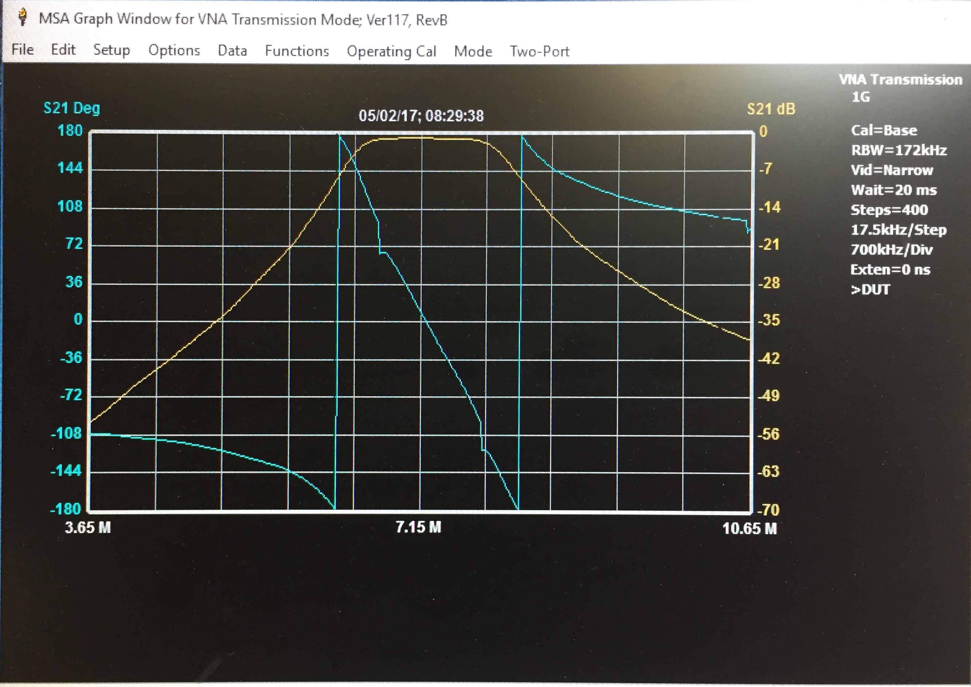
The measured PA performance with this transformer are actually quite good:

 
(glitch in the first curve is likely due to the FW issue described by Steve, did not yet update to the latest version)
The high frequency response is even improved, which I did not expect. The transformer did not get too hot even at 5 W out for some (relatively) long periods at 1.8 MHz and 29 MHz. Harmonics also look fine.

I think similar results could be obtained with a BN-43-1502, which has similar dimensions, with double the number of turns but I do not have one at hand to try now.


73 de Claudio, IN3OTD / DK1CG

On Tuesday, May 9, 2017 at 11:06:48 PM UTC+2, Takashi K wrote: Hi Steve,

Takashi K

unread,
May 12, 2017, 7:46:57 AM5/12/17
to Hermes-Lite
Hello Claudio,

Thanks for your experiment.
That's a nice solution !  I think that IMD will be improved a bit as well.
I'd like to recommend to use this TDK core as HL2 standard component.

73, Taka  ji1udd

Graeme Jury

unread,
May 13, 2017, 7:05:28 PM5/13/17
to Hermes-Lite
Takashi san konnichi wa,

Sorry to be so long replying but I have been away and have now returned. I think the solution from Claudio is perfect for you and looks to have performance advantages as well. I am happy to try to do a cutout if you wish to continue that way but with complete sets of filters there will be very little board space.

73, Graeme yori

Takashi K

unread,
May 13, 2017, 9:07:11 PM5/13/17
to Hermes-Lite
Hello Graeme san,

Thanks for your reply. I'm satisfied with Claudio's solution. So no need to consider a cutout now.
I'm looking forward to HL2 filter board.

73, Taka ji1udd

Steve Haynal

unread,
May 14, 2017, 2:16:45 AM5/14/17
to Hermes-Lite
Hi Claudio,

This looks like a nice short alternative. I've been noticing that my BN-43-202 has been getting hot during QSO TX. This is one of the few parts that will probably have to be assembled by the user at least for the first 50 or so units. I was planning on just including a BN-43-202 in each order but can substitute this or similar part. The TDK part is 3x the cost of a BN-43-202. Do you know of a good supplier where I can purchase ~50 for less money?

73,

Steve
KF7O

in3otd

unread,
May 14, 2017, 3:23:25 AM5/14/17
to Hermes-Lite

Hello,
I remember that the BN43-202 sometimes was getting a little hot on the testPA board, for the H-Lv2b2 I've always run all the tests with a small fan usually, actually mainly because of the lack of a proper heatsink for the PA, so I didn't notice this. A transformer with a BN61-202, with twice the number of turns, was running cooler.
I don't know of any other sources for that TDK binocular core, I bought mine from Digikey some time ago but I see they are now out of stock there (and they are not cheaper anyway). Still is not clear why the upper HF response is improved, maybe due to less leakage inductance.


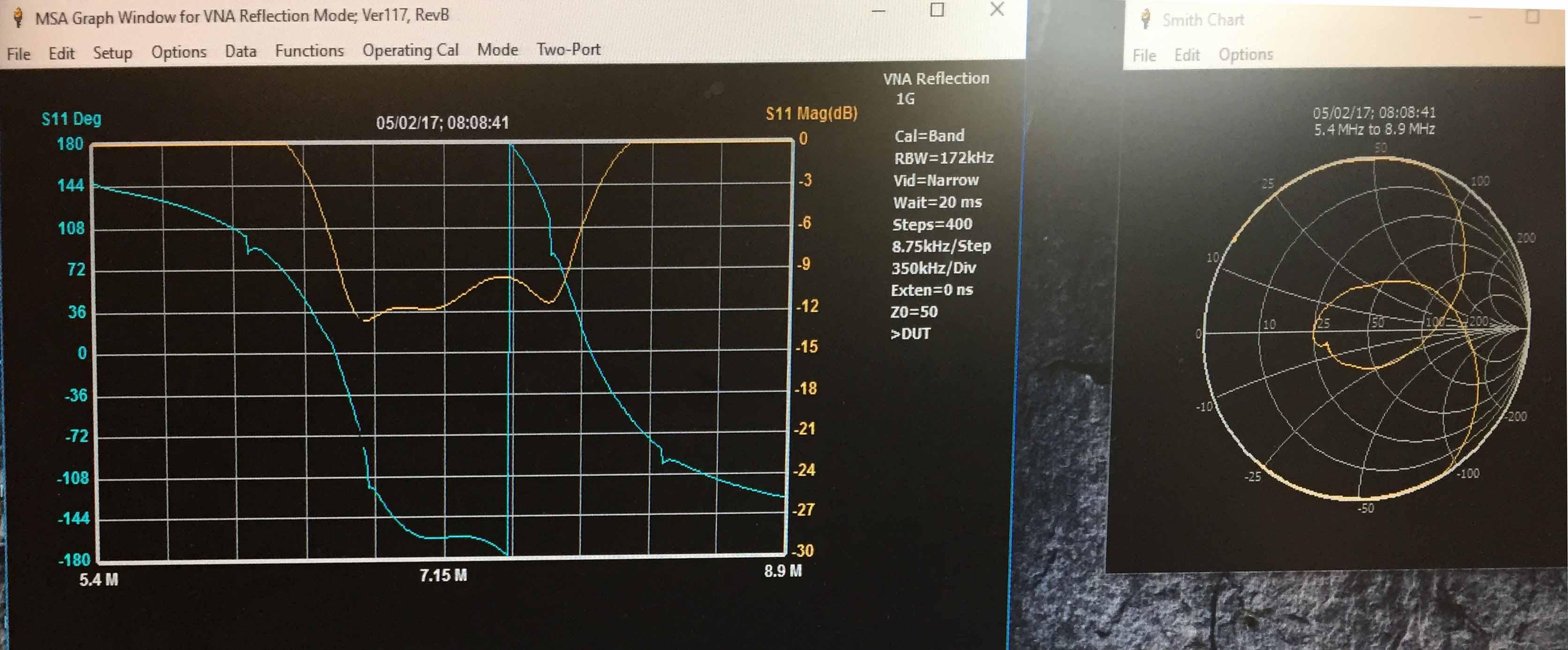
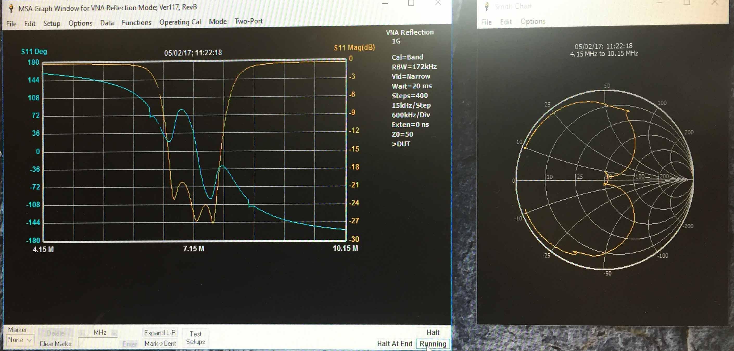
Also the IMD performances look significantly better:


which is also "suspect"; I'll try to do some more experiments.

BTW, I've now the H-Lv2b2 in the 105x100 enclosure (black version) but a bit disappointed by its heatsinking performance: with 5 W out the PA thermal sensor goes above 50 C after just a few seconds. I'll try to add a copper strip soldered to the PCB border as in your pictures.


73 de Claudio, IN3OTD / DK1CG

Takashi K

unread,
May 14, 2017, 5:08:51 AM5/14/17
to Hermes-Lite
Hello,

Steve,
Arrow Electronics has 557 pcs in stock now.  And price is a little bit lower than Digikey.
1+   $0.9826
10+  $0.8469
100+ $0.5518

Claudio,
Thanks for your additional mesurement. Very good IMD !

73, Taka  ji1udd


Steve Haynal

unread,
May 15, 2017, 2:04:31 AM5/15/17
to Hermes-Lite
Hi Claudio,

Regarding heat sinking with the black case, do you have a nut and bolt in place to provide some force on the PCB push it firmly on the slot edge? I have stopped using the copper strip as just the nut and bolt appear to be adequate. I am using natural aluminum which may be better for heat transfer. I just ordered a black case to see how it behaves for me. I am also using only 8V for the PA. Are your temperature measurements from the slow ADC as reported by Quisk?

I rarely see the temperature go above 50C. Maybe after 1 or 2 minutes of JT-9 or WSPR TX into an antenna with a SWR of 2 up to 3 to 1 it will reach the low 50C range. Usually it always remains in the 40C range.

73,

Steve
KF7O

Takashi K

unread,
May 20, 2017, 10:54:36 PM5/20/17
to Hermes-Lite
Hi Steve,

I'm planning to make power control board for my HLv2 compact tranceiver. See the attached circuit(pdf).
I'd like to control HLv2 and RPi/LCD power individually by PIC micon.
Could you add a jumper (0 ohm resistor) and a terminal ( DBxx ) for using EN of U3 and U16 as user option.
If there is not enough space for DBxx, I use the jumper pad (EN side) to connect control signal.

73, Taka  ji1udd

PowerControl_v10.pdf

in3otd

unread,
May 23, 2017, 3:28:35 PM5/23/17
to Hermes-Lite

Hello,
initially I used a big clamp to push the PCB down on the slot edge, then I tried to put something below the PCB instead, to push it to the slot upper edge and finally I also tried without any clamp or other and did not actually see much difference in the measured temperature in TX. On my PCB the tinned edges may not be perfectly flat anymore since I did some soldering there before but I cleaned them up after and I think they should make a good contact anyway.


I've also tried putting a small aluminum block below the PA area, with a piece of Kapton tape to avoid short circuits


the PCB+aluminum block was then forced in the enclosure; the temperature during TX is now lower but still rising too fast, IMHO. I'll try to do some more measurements.

The temperature was measured using the slow ADC via Quisk, after tuning the formula to match the voltage read on the temperature sensor with a multimeter.


73 de Claudio, IN3OTD / DK1CG


On Monday, May 15, 2017 at 8:04:31 AM UTC+2, Steve Haynal wrote:
Hi Claudio,

Steve Haynal

unread,
May 27, 2017, 2:31:37 AM5/27/17
to Hermes-Lite
Hi Claudio,

I received my black enclosure and did some comparison tests with the raw aluminum enclosure. All tests were at full power. I measure 7.5W on my scope without any filter into this dummy load. The signal was generated with Quisk spot on 20M, full amplitude for the spot and full amplitude for the TxDAC control. The ambient temperature was 27C in a large closet with little air circulation. The test lasted 5 minutes and I took a temperature reading via Quisk every 30 seconds. Quisk was calibrated for my 3.268V supply. I run the PA at 8V not 9V. This may be why I see less heating. Only a screw, washer and bolt were holding the PCB down in the enclosure slot. Only half of the enclosure was used, no top or end plates.

Raw Aluminum
33.0
44.0
46.0
47.0
48.0
49.0
49.7
50.2
51.0
51.5
52.1

Only after 3 solid minutes did it hit 50C. Just before the end, I felt the transistors and they were hot but did not burn my finger. I did burn my finger on the dummy load...  I tried with the other half of the enclosure in place and found the temperatures were actually about a degree higher by the end.


Black Enclosure Test 1
33.5
49.3
52.0
54.0
55.2
56.0
57.0
57.7
58.3
58.8
59.5

The black enclosure is not as good. I had about the same force from the nut and screw as in the last test. I sanded the slot slightly for a second test.

Black Enclosure Test 2 with sanded slot
31.0
47.1
50.1
51.9
53.0
54.0
55.0
55.8
56.4
57.0
57.5

Still not as good as the raw aluminum, and the initial temperature was lower. Again I felt the LDMOS transistors with my finger just before the end and I wasn't burnt. It actually reminded me of how hot my FT817ND sometimes felt.

I think the raw aluminum enclosure is adequate, but we have yet to test in the Australian outback on a hot summer day... The HL2 has current and temperature sensing and firmware will reduce or shutoff transmit if we are approaching any limits. I think we are safe.


73,

Steve
KF7O


Steve Haynal

unread,
May 27, 2017, 3:02:58 PM5/27/17
to Hermes-Lite
Hi Claudio and Group,

I was taking a close look at my two enclosures today and noticed that the PCB slot is not necessarily flat. I tried to take pictures but they didn't turn out well. In my black enclosure the PCB slot is narrower at the top but wider at the bottom. This means only a narrow "lip" not the ideal 1.5mm to 2mm will make contact with the PCB when the PCB is pressed down. In my natural enclosure, the slot width from top to bottom is much more uniform and more of the case will make contact with the PCB when the PCB is pressed down. Besides possible thermal transfer differences in the various coatings, this could be a factor in the differences we are seeing between various enclosures.

I don't think slot flatness is a tolerance that manufacturers care about or control much in these inexpensive enclosures. I am beginning to worry that we'll see lots of heat variation among enclosures due to this. If you are lucky and your enclosure has a fairly flat slot like mine, then dissipation can work pretty well.

I will contact some manufacturers to learn more and also ask/order some 100mm length enclosures. 

73,

Steve
KF7O

in3otd

unread,
May 27, 2017, 4:40:46 PM5/27/17
to Hermes-Lite
Hello Steve,
out of curiosity, is your "natural aluminum"  enclosure really uncoated/non-anodized/raw? I've seen on ebay that these are sometimes also described as "powder coated" and seems not so shiny as, e.g., the typical non-anodized heatsink.
The slots in my black enclosure look quite flat, except for the first centimeter or so at the extremities, where the slots were evidently deformed when creating the threads for the front screws. Maybe some amount of thermal compound could help anyway.


73 de Claudio, IN3OTD / DK1CG

Steve Haynal

unread,
May 28, 2017, 2:18:26 AM5/28/17
to Hermes-Lite
Hi All,

I receive responses directly to me but will answer here.

Pete, yes Hammond cases are a possibility. There a bit of work in tracking on down with the correct dimensions. We need one that is in the range of 95 to 100 mm wide and 100 to 103 mm in length. Ideally we want enough vertical room for two boards, 3+ cm spacing between the boards.

John, yes thermal grease is something I've wanted to try, but I always make a mess when I use it! The attached data has some experiments with thermal grease and it does help some.

Claudio, I went back and checked the vendors description but am still not 100% certain regarding any coating on my natural aluminum enclosure. It passes the electrical conductivity test so I don't think it is anodized. It doesn't appear to have any powder coating. I believe it is "mill finish." Search for AK-C-C12. Are you using 8V or some other voltage for the PA? As your measurements indicated, dissipated power is less for the lower supply in the 7.5 to 8V range.

I tried adding the side plate idea again to the black enclosure, but this time I "smashed" some copper desoldering braid down on the tabs. See the attached picture. The idea was that this would make better thermal contact with the irregular solder covered tab surfaces. I also sanded off most of the black coating underneath the copper plate. The slide plate is bolted in such a way that it is pushing down on the PCB. This worked quite well and I see thermal profiles similar to what I was seeing with the natural aluminum case. See the attached data with Side Plate==Y.

Next I added some thermal grease and results improved some more by about a few degrees. I switched back to the "Bottom Screw" but with thermal grease and this appeared to make a large difference compared to my initial measurements. I double checked power output. This was at a hotter time of day and after several measurements so I would have expected temperatures to be higher. I combined all techniques and did not see temperatures greater than 50C for the black enclosure and 45C for the natural enclosure. The natural enclosure still appears better and results for it were also improved by these techniques.

For comparison, the data also has 3 back to back WSPR transmits into a 20M antenna with a SWR of ~2.5:1. With this mismatch you can see that more power must be dissipated. Also, after each 1 minute 50 seconds WSPR stops transmitting for 10 seconds and you can see the temperatures drop in the data.

I wanted to understand better how accurate the onboard temperature sensor is. I wired up a second sensor and my wife held it and the ground lead firmly on the case of one LDMOS device while I ran a TX experiment. The second sensor was reading about 1 degree C less than the onboard sensor (these sensors may be off by 4C but will track well once calibrated). During TX that difference went down to 0.6 to 0.8 degrees and tracked well. This makes me believe we have good readings from the onboard sensor.

If an AFT05MS003N device is dissipating 5W (this is on the high side), then the difference in temperature between the case and junction is 4.1*5= 20.5C. For errors and fudge factors, let us assume 30C difference between the actual junction temperature and the reading from the sensor. The AFT05MS003N can operate up to 150C junction temperature although MTBF may increase. I do not see temperatures even near 150-30=120C from the sensor. We have plenty of headroom and as safety the firmware can start turning down TX power at 70C and power off TX at 80C and still be well below the max. So even if we see variations of 10C to 15C between enclosures, I think it is still okay.

73,

Steve
KF7O


HL2 Temp Measurements - Sheet1.pdf

in3otd

unread,
Jun 4, 2017, 3:36:31 AM6/4/17
to Hermes-Lite

Hello Steve,
thanks for the measurements; I'm still using the 9.4 V supply for the PA so this may be part of the reasons I see higher temperatures.
I did some more measurements with my black case: with just the "bottom screw" and with the aluminum block, transmitting at 5 W out for 60 seconds:


interestingly, with the aluminum block the temperature went actually higher: I think it may have not been well positioned and touched some of the nearby SMD components, so not making good contact with the PCB. Adding thermal grease improved things quite a bit but I was hoping to be even better. One problem with the Al block is that the PCB borders do not have a good contact with the enclosure side slots anymore.
In the meantime I ordered and received a "natural aluminum" box (finish actually described as "surface sandblasting, brushed processing") but had no luck and got a box with a non conductive coating, probably still powder coated as the black enclosure I have.


73 de Claudio, IN3OTD / DK1CG


Steve Haynal

unread,
Jun 5, 2017, 2:11:04 AM6/5/17
to Hermes-Lite
Hi Claudio,

Interesting measurements. I plan to eliminate some through holes and nudge a few components in the PA area so that it will be easier to use an aluminum block like you are experimenting with. Those wishing to use TO220 devices will have to bend some leads and solder to just top pads. See  https://github.com/softerhardware/Hermes-Lite2/issues/37

regarding enclosures. I plan to order four cases 101mm length for beta3.

73,

Steve
KF7O
Reply all
Reply to author
Forward
0 new messages