Design blog for 10-in-1 multi-function board for RC2014
340 views
Skip to first unread message

Bill Shen
Jun 4, 2021, 3:22:32 PM6/4/21
to retro-comp
It is well known that you can order 10 100mmX100mm pc boards from China for $5. This is the motivation for designing one pc board for RC2014 that can have 10 different functions. Another word, by populate with different components, jumpers, and different firmware, such multifunction pc board can perform 10 different functions. Since it is for RC2014, a board size of 50x100mm with through-hole components is desirable.
The design I'm thinking of is based on the Frugal RAM/ROM 512K board. It already has multiple functionalities so I'm thinking of adding more to the list:
1. RAM/ROM 512K with CF interface and I2C interface
2. Emulated 6850 serial port
3. Second CF interface
4. Clock & reset supervisor
5. EPROM programmer
6. Discrete inputs and output LEDs
7. 4x40 LCD display
8. Six 7-segment displays
9. SPI & I2C interface
10. Diagnostic board
The design revolves around a CPLD that can be programmed for different functions. Multiple components occupy the same pc board location but only one is populated for a given board function. Jumpers may be needed to enable/disable certain functionalities. This is really 10 separate designs, so a few iterations are needed to get them all correctly. I hope to implement all 10 functions after 2-3 iterations of board design. The design will be open hardware so anyone can order their own pc boards.
This is the design blog for the 10-in-1 board. I expect it to go on for a while since several iterations of the 10 designs will be described in this blog.
Bill
Bill Shen
Jun 6, 2021, 10:48:54 PM6/6/21
to retro-comp
FRR512K
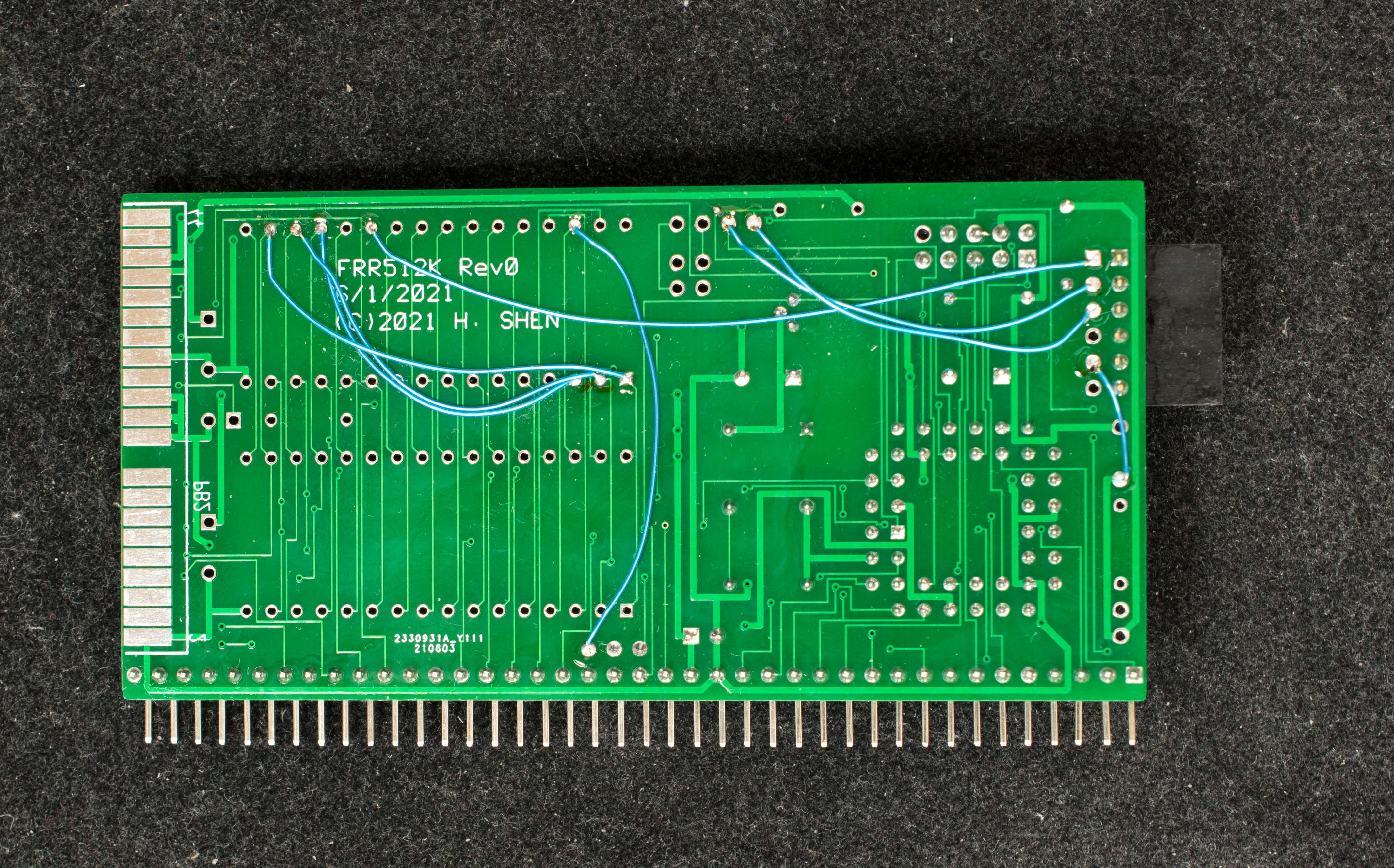
The first iteration of 10-in-1 board is a repurposed FRR512K board. With few jumpers added and changes in CPLD equations, functions 1 thru 5, 9 and 10 can be achieved with rev0 of FRR512K board. Attached is board layout and schematic of rev0 of FRR512K. The pc boards are on their way from JLCPCB to me.
The testbed is a 5-slot RC2014 backplane, Karlab's #23c (Z80 and 7.37MHz clock), and Karlab's #32b (68B50 ACIA). FRR512K will be configured to function 1 (RAM/ROM 512K with CF and I2C) which is its intended design. The resulting 3-board system should run ROMWBW and boot into CP/M with CF drive at 7.37MHz.
Bill
Bill Shen
Jun 9, 2021, 8:45:42 PM6/9/21
to retro-comp
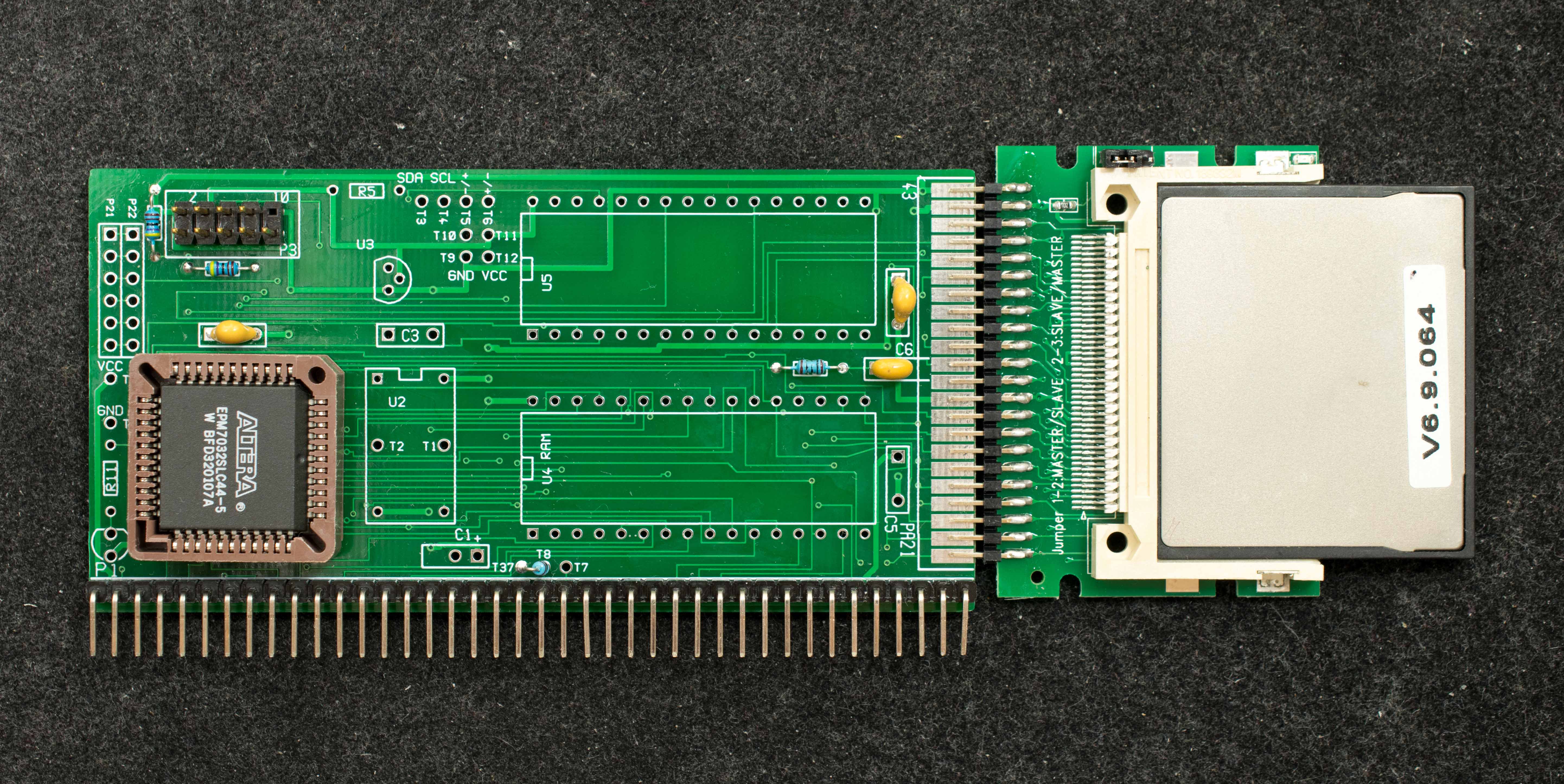
Function 1, part 1, RAM/ROM512K
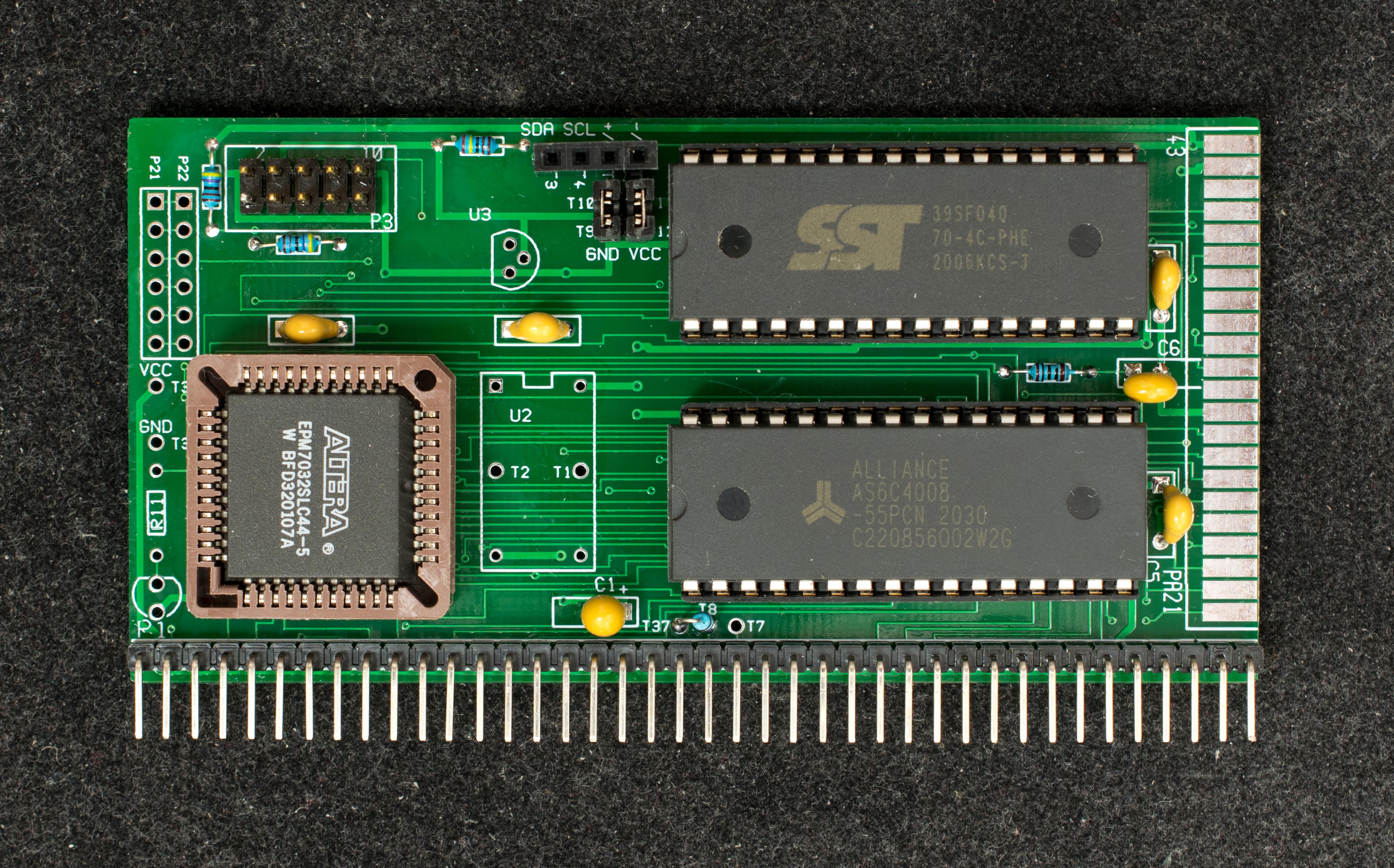
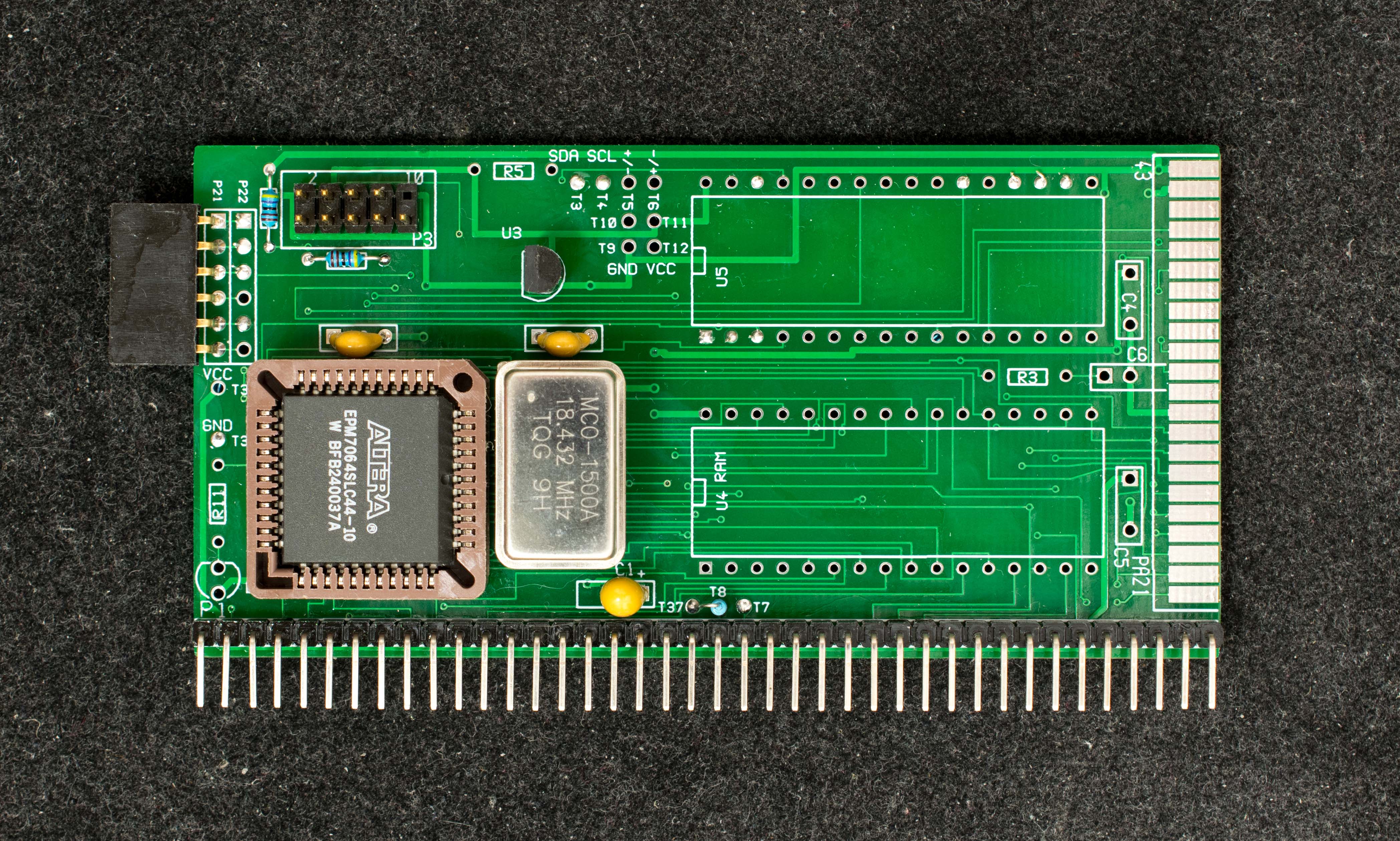
Received the pc boards from JLCPCB this morning (I sent off the design last Wednesday and received the board today, Wednesday). I populate it with its intended design function which is RAM/ROM 512K with CF interface and I2C. The picture shows the board in its most basic configuration which is just 3 chips--RAM, ROM and CPLD without the CF interface. In this basic configuration plus Karlab's #23 (Z80 + clock) and Karlab's #32b (68B50 ACIA), it is able to boot up ROMWBW. This mirrors the function of the original RC2014 512K ROM 512K RAM board.
Bill

Wayne Warthen
Jun 9, 2021, 9:12:21 PM6/9/21
to retro-comp
That's impressive Bill. Nice work.
-Wayne
Bill Shen
Jun 10, 2021, 8:55:56 PM6/10/21
to retro-comp
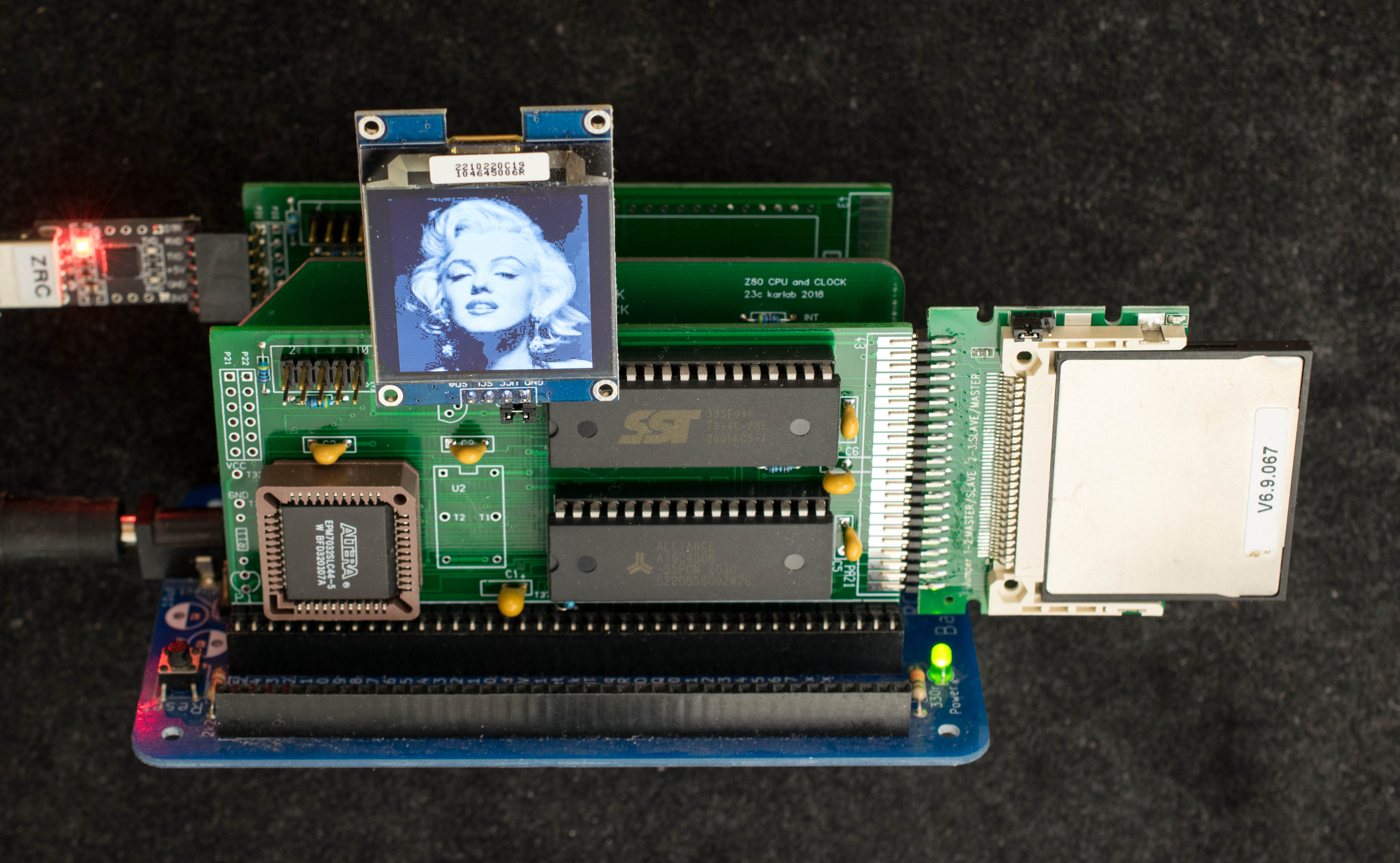
Function 1, part 2, RAM/ROM512K with CF interface and I2C
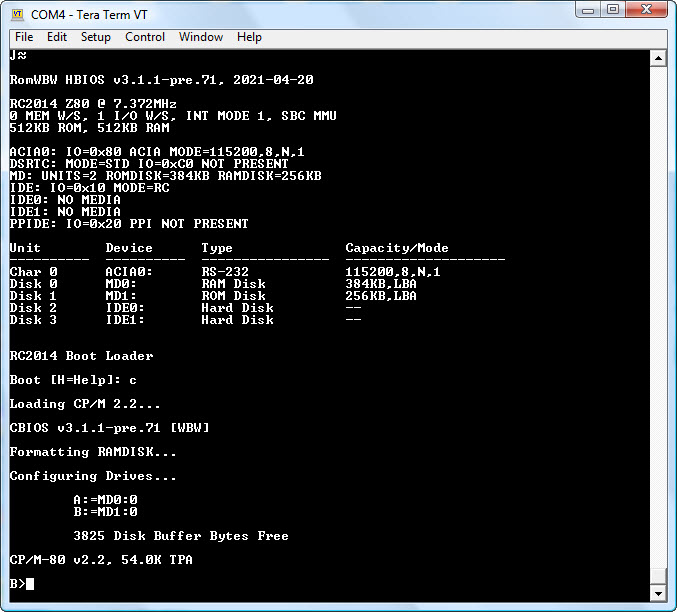
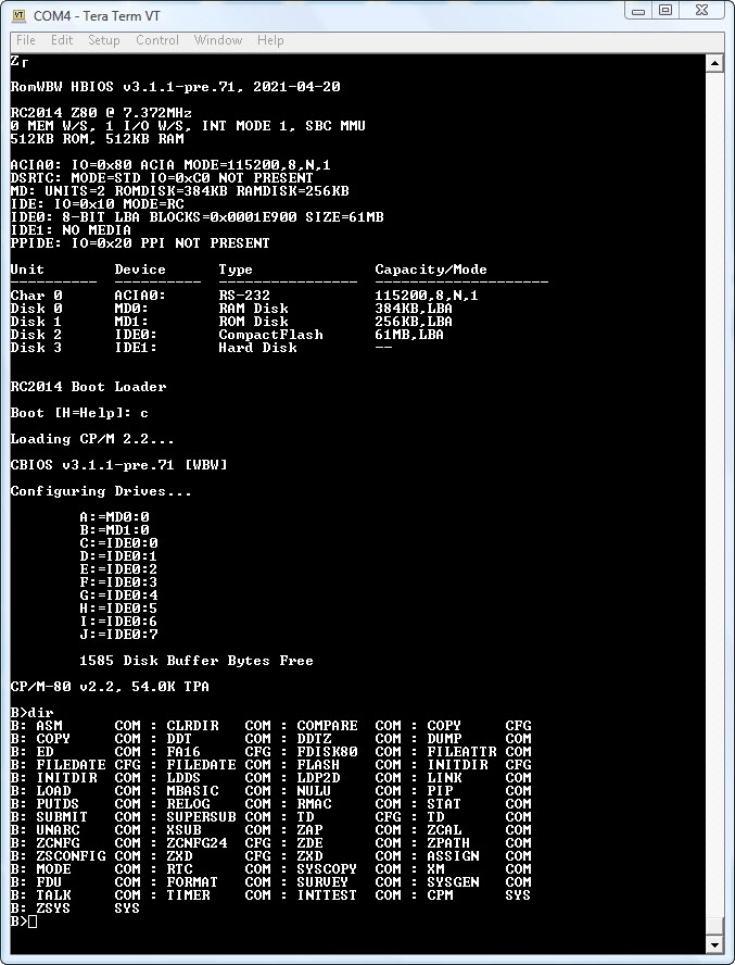
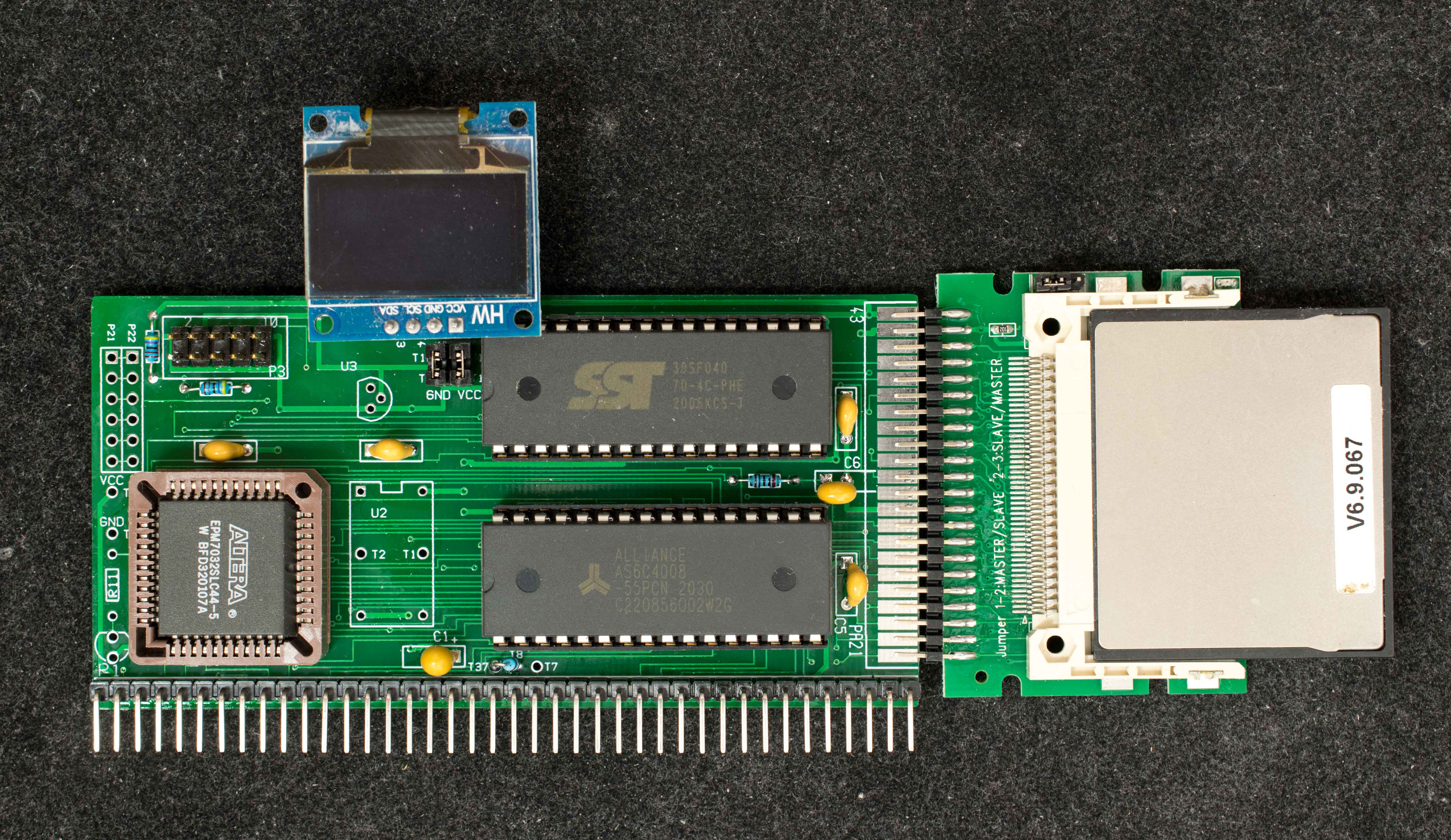
Here is the completed FRR512K with CF interface and I2C. CF interface is located at the default I/O addresses of 0x10-0x17 so ROMWBW autodetects it and enables the CF interface as IDE0. I can copy with verify the content of ROM drive (drive B:) to drive C: so the CF interface appears to work.
I2C also works. It is a simple bit-bang interface; I ran Game of Life and measured data transfer rate at about 8Kbytes/sec with 7.37MHz CPU clock. The 128x64 OLED display needs 1K bytes of data to fill the display so this translates to 8 frames/sec, max. I think there are things I can do to raise the screen fill rate to 20 frames/sec, fast enough to display animated GIF at correct speed. I'll come back to faster I2C later, but right now I'm going forward to Function 2, emulation of 6850 serial port.
Bill

Interocitor Steve
Jun 11, 2021, 1:56:49 PM6/11/21
to retro-comp
Looks awesome, Bill. I like the little display. My Planet Locator App will probably use an OLED display.
BTW, what is a CF? Is that a memory card slot?
=Steve.

Terry Fox
Jun 11, 2021, 2:46:00 PM6/11/21
to retro-comp
CF is Compact Flash, the square card on the right side in the picture. It is/was used a lot in digital cameras. The advantage of it is that it can use a multi-bit parallel interface, I think similar to the IDE standard. Several single board retro computers use CF cards.
Terry, N4TLF
Bill Shen
Jun 11, 2021, 7:36:13 PM6/11/21
to retro-comp
Steve,
Like Terry Fox said, CF stands for Compact Flash. The IDE-44 connector on the right edge of the PC board can accept a CF adapter directly or a ribbon cable to the old fashion spinning disk hard drives.
The OLED display in previous picture is a small (0.96") 128x64 black & white display. The pixels are either on or off, there are no color or grey scale. You may want to consider a larger (1.5") 128x128 16-level grey scale display that still can be driven with I2C interface. However, it takes 8Kbytes of data to fill the screen so faster data transfer rate is a must. There are also color OLED displays, but use SPI interface and I have no experience with them.
Bill

Mark T
Jun 11, 2021, 11:11:28 PM6/11/21
to retro-comp
Has anybody confirmed the simple compact flash interface can drive an IDE hard drive? I have an old 1.8” IDE drive that might be a good candidate if there is a chance of this working.
One possible way to speed up a bit banged serial interface might be to buffer the high address lines shifted by one bit to the data lines, then an IN instruction can input one bit and shift the accumulator, an unrolled loop of eight inputs could provide serial input and/or output of a byte. Unfortunately it looks like you don’t have enough pins on the cpld to try this.

Phillip Stevens
Jun 11, 2021, 11:15:30 PM6/11/21
to retro-comp
Mark T wrote:
Has anybody confirmed the simple compact flash interface can drive an IDE hard drive? I have an old 1.8” IDE drive that might be a good candidate if there is a chance of this working.
It would only work if is 16 bit enabled. Otherwise only XT-IDE drives (ancient 8-bit interface) would work on a CF interface.
Bill Shen
Jun 12, 2021, 11:04:20 AM6/12/21
to retro-comp
I do know some users of my boards have successfully attached spinning disk hard drive to the IDE44 connector. I have not done it myself. I'll dig out my old PATA drives and give that a try. It should work; the "set feature" command is part of the ATA spec which set the 16-bit data bus to 8-bit data. Even if the set feature command is not implemented, I can use the lower 8-bit and ignore the upper 8-bit of the 16-bit bus. It is wasteful of storage space since only 50% is utilized and sector size becomes 256 bytes instead of 512 bytes, but then CP/M can only use 128Meg of a disk anyway.
Bill
Bill Shen
Jun 12, 2021, 1:01:13 PM6/12/21
to retro-comp
Function 2, CPLD emulation of 6850 ACIA
The core ACIA functionalities can be emulated with a modest 64-macrocell CPLD like EPM7064S (ATF1504). It does not emulate all functions, but enough so ROMWBW will see it as the 6850 ACIA. Attach is the schematic of the emulated 6850. It has no error handling capabilities, the status register only reports transmit empty and receive full flags. It does have the interrupt function as well as RTS handshake. Software reset will yield the correct status data so ROMWBW will detect its presence at I/O addresses at 0x80/0x81 and 0xA0/0xA1.
To emulate the RC2014 ACIA board, only CPLD and the serial connector need to be installed. Jumpers need to be added to bring all 8 data bits to CPLD, serial transmit/receive/handshake to the serial connector and interrupt to RC2014 bus. This is a good place to include oscillator/reset supervisor function because the emulated ACIA can run much faster than 7.37MHz, so clock can be increased to the limit of EPROM/RAM access time. 18.4MHz is the nominal frequency of Z80180 RC2014 systems so it may be desirable to operate Z80 system at 18.4MHz as well. Last picture shows a 18.4MHz ROMWBW system consists of a Z80 CPU, emulated 6850 with 18.4MHz oscillator, and a FRR512K board with CF disk and I2C.
On Friday, June 4, 2021 at 1:22:32 PM UTC-6 Bill Shen wrote:

Alan Cox
Jun 12, 2021, 3:33:56 PM6/12/21
to Bill Shen, retro-comp
On Sat, 12 Jun 2021 at 16:04, Bill Shen <coinst...@gmail.com> wrote:
I do know some users of my boards have successfully attached spinning disk hard drive to the IDE44 connector. I have not done it myself. I'll dig out my old PATA drives and give that a try. It should work; the "set feature" command is part of the ATA spec which set the 16-bit data bus to 8-bit data. Even if the set feature command is not implemented, I can use the lower 8-bit and ignore the upper 8-bit of the 16-bit bus. It is wasteful of storage space since only 50% is utilized and sector size becomes 256 bytes instead of 512 bytes, but then CP/M can only use 128Meg of a disk anyway.
The 8bit set feature is a CF specific command. It's not required on anything that isn't CF (although to confuse things there are of course rotating disks that are CF compliant like the IBM microdrive). Depending what lines and spre you have in the logic there are a few ways to handle this. Many of the adapters for old micros use A8 to select between an 8bit latch and the CF data bus. For output (less common) you can write latch/data latch/data. For input inir toggles A8 and you get full speed data/latch/data/latch
Alan

Nigel Kendrick
Jun 12, 2021, 4:20:10 PM6/12/21
to retro-comp
Bill Shen
Jun 25, 2021, 9:07:40 PM6/25/21
to retro-comp
Function 3, 2nd CF disk
The CPLD design for 2nd CF disk is very simple; it is the same CF design as the original FRR512K except the I/O base address is changed to 0x20. It uses 7 macrocells out of 32 available, so there are plenty of room available for other functions, such as I2C or SPI, or combines with 6850 serial port emulation function.
To enable the 2nd CF disk at 0x20, it is necessary to add the configuration statements to RCZ80 as described by Wayne Warthen here and burn a new EPROM:
IDECNT .SET 2 ; IDE: NUMBER OF IDE INTERFACES TO DETECT (1-3), 2 DRIVES EACH
IDE1MODE .SET IDEMODE_RC ; IDE 1: DRIVER MODE: IDEMODE_[DIO|DIDE|MK4|RC]
IDE1BASE .SET $20 ; IDE 1: IO BASE ADDRESS
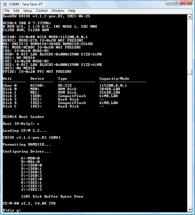
This is the bootup display where drive C-F are the first CF disk and drive G-J are second CF disk. It all works very well.
Bill
The CPLD design for 2nd CF disk is very simple; it is the same CF design as the original FRR512K except the I/O base address is changed to 0x20. It uses 7 macrocells out of 32 available, so there are plenty of room available for other functions, such as I2C or SPI, or combines with 6850 serial port emulation function.
To enable the 2nd CF disk at 0x20, it is necessary to add the configuration statements to RCZ80 as described by Wayne Warthen here and burn a new EPROM:
IDECNT .SET 2 ; IDE: NUMBER OF IDE INTERFACES TO DETECT (1-3), 2 DRIVES EACH
IDE1MODE .SET IDEMODE_RC ; IDE 1: DRIVER MODE: IDEMODE_[DIO|DIDE|MK4|RC]
IDE1BASE .SET $20 ; IDE 1: IO BASE ADDRESS
This is the bootup display where drive C-F are the first CF disk and drive G-J are second CF disk. It all works very well.
Bill
On Friday, June 4, 2021 at 1:22:32 PM UTC-6 Bill Shen wrote:
Reply all
Reply to author
Forward
0 new messages