A Frugal CPLD-based 512K ROM/RAM board for RC2014, a design blog
434 views
Skip to first unread message

Bill Shen
May 14, 2021, 6:32:28 PM5/14/21
to RC2014-Z80
This is a design blog for a frugal CPLD-based 512K ROM/RAM board. It is a spin-off of this topic: https://groups.google.com/g/rc2014-z80/c/f1KBSsxsic8
The keyword is "frugal"; this design is a consolidation of all TTL logic into a 32-macrocell CPLD (556-AF1502ASV15JU44) which can be purchased at Mouser for $1.88 in quantity of 1.
This is a design blog tracking a design from concept to pc board.
Bill
The keyword is "frugal"; this design is a consolidation of all TTL logic into a 32-macrocell CPLD (556-AF1502ASV15JU44) which can be purchased at Mouser for $1.88 in quantity of 1.
This is a design blog tracking a design from concept to pc board.
Bill
Bill Shen
May 14, 2021, 6:57:30 PM5/14/21
to RC2014-Z80
Introduction
The original 512K RAM/ROM is documented here: https://rc2014.co.uk/modules/512k-rom-512k-ram-module/
The frugal CPLD version will have 3 IC:
1. 512K RAM, AS6C4008
2. 512K EPROM, ST39SF040
3. ATF1502ASV15JU44 or its equivalent, EPM7032SLC44
The design is based on Wesley Isacks' simplified version of 512K RAM/ROM where memory bank is 32K instead of 16K. The CPLD will be under utilized so it should have spare logic for a compact flash interface and additional functions such as I2C interface. The design should be capable of supporting 14.7MHz Z80, possibly 22MHz.
The prototype vehicle is ProtoRC3 which has a CPLD in 44PLCC socket interfaces to the 39-pin RC2014 bus. https://www.retrobrewcomputers.org/doku.php?id=builderpages:plasmo:protorc3 It also has a footprint for an IDE44 connector to support a CF interface. The 512K RAM and EPROM fit in the prototype area.
The nature of designs based on CPLD are such that PC board design or prototyping can be started in parallel with the logic design. So the first step is placing the EPROM and RAM on the prototype board and wire them up and worry about logic design later.
Here we go...
Bill
Bill Shen
May 15, 2021, 8:01:50 PM5/15/21
to RC2014-Z80
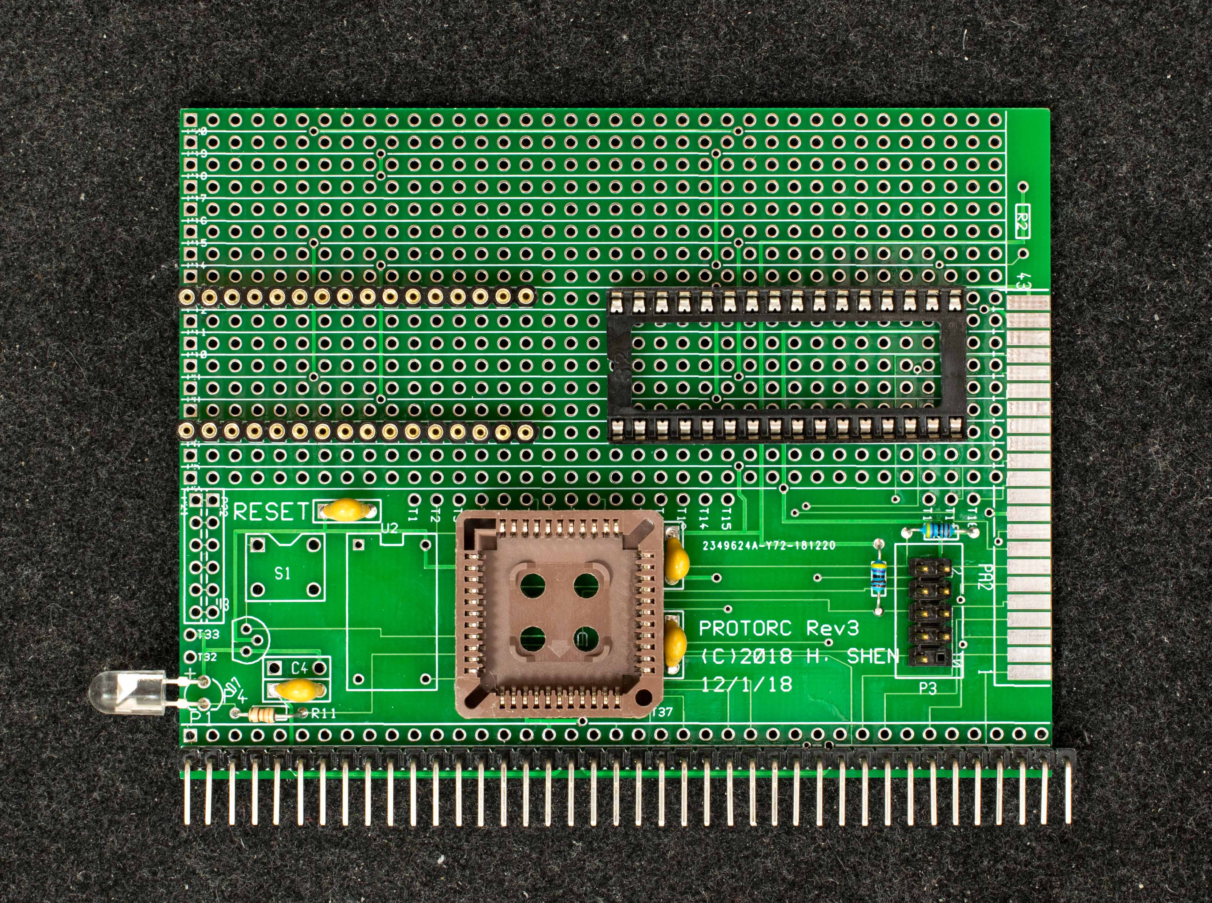
Prototype layout
The component layout of the prototype frugal 512K RAM/ROM is straightforward. EPROM is at top left with machine socket so it can be removed easily. RAM is top right. CPLD is housed in a PLCC socket at bottom center with the Altera CPLD programmer header at bottom right.
Attached is schematic of the prototype FRR512K
Bill
On Friday, May 14, 2021 at 4:32:28 PM UTC-6 Bill Shen wrote:
Bill Shen
May 16, 2021, 5:18:49 PM5/16/21
to RC2014-Z80
Prototype
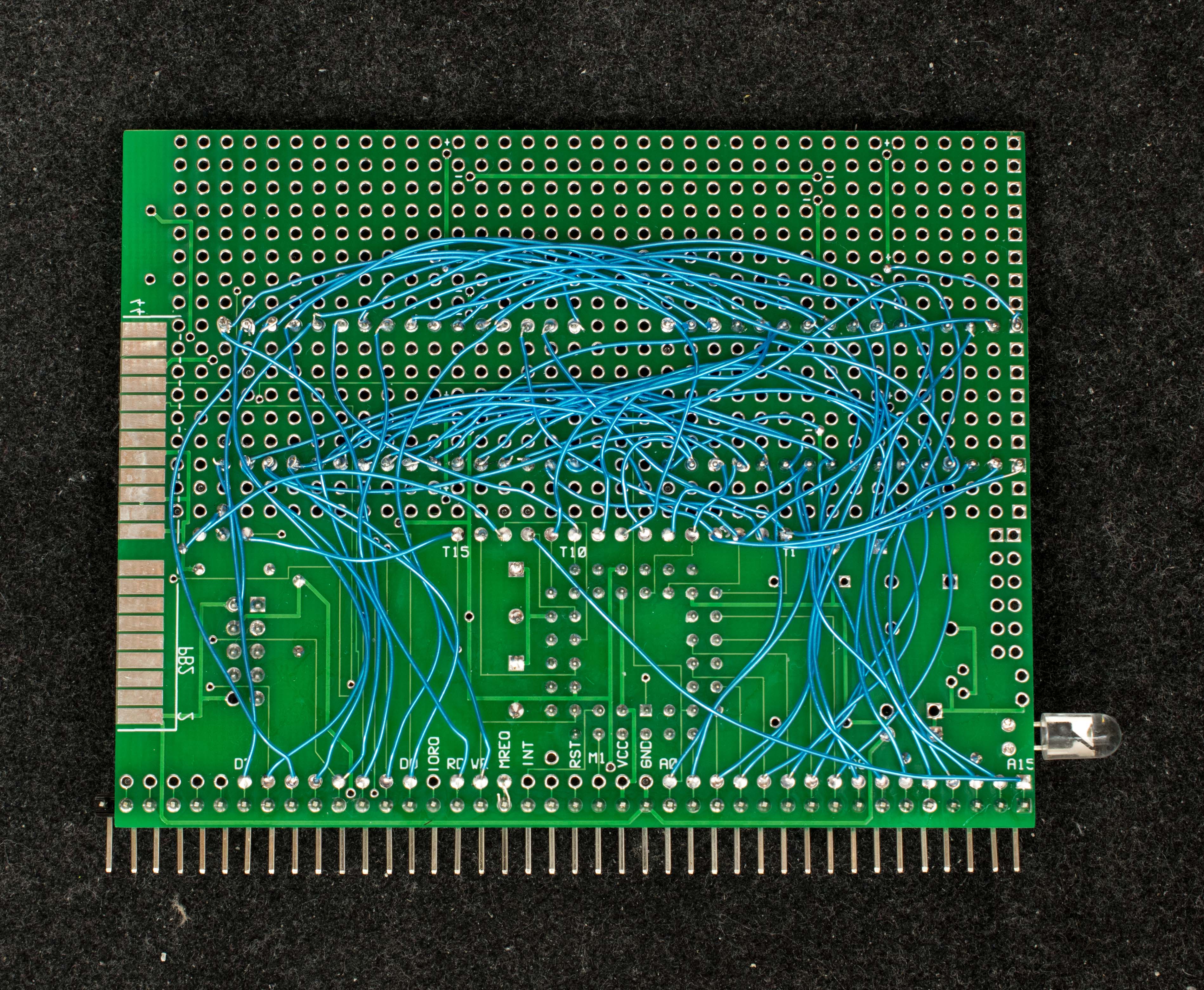
The prototype board is all wired up using point-to-point wiring. Wire wrapping is easier but wire wrap sockets are harder and harder to find AND expensive, especially for the PLCC socket. For small projects, point-to-point wiring is not too tedious.
The component side is populated for the camera. In real life, CPLD is first populated and programmed before EPROM and RAM are populated.
Now I'm ready to port Wesley Isacks' logic design to the CPLD.
Bill
On Friday, May 14, 2021 at 4:32:28 PM UTC-6 Bill Shen wrote:

William Huskey
May 16, 2021, 5:22:54 PM5/16/21
to RC2014-Z80
Nice sir..
--
You received this message because you are subscribed to the Google Groups "RC2014-Z80" group.
To unsubscribe from this group and stop receiving emails from it, send an email to rc2014-z80+...@googlegroups.com.
To view this discussion on the web, visit https://groups.google.com/d/msgid/rc2014-z80/b8da100c-8640-4132-88dd-155ae4a0f1ddn%40googlegroups.com.
Bill Shen
May 16, 2021, 8:18:11 PM5/16/21
to RC2014-Z80
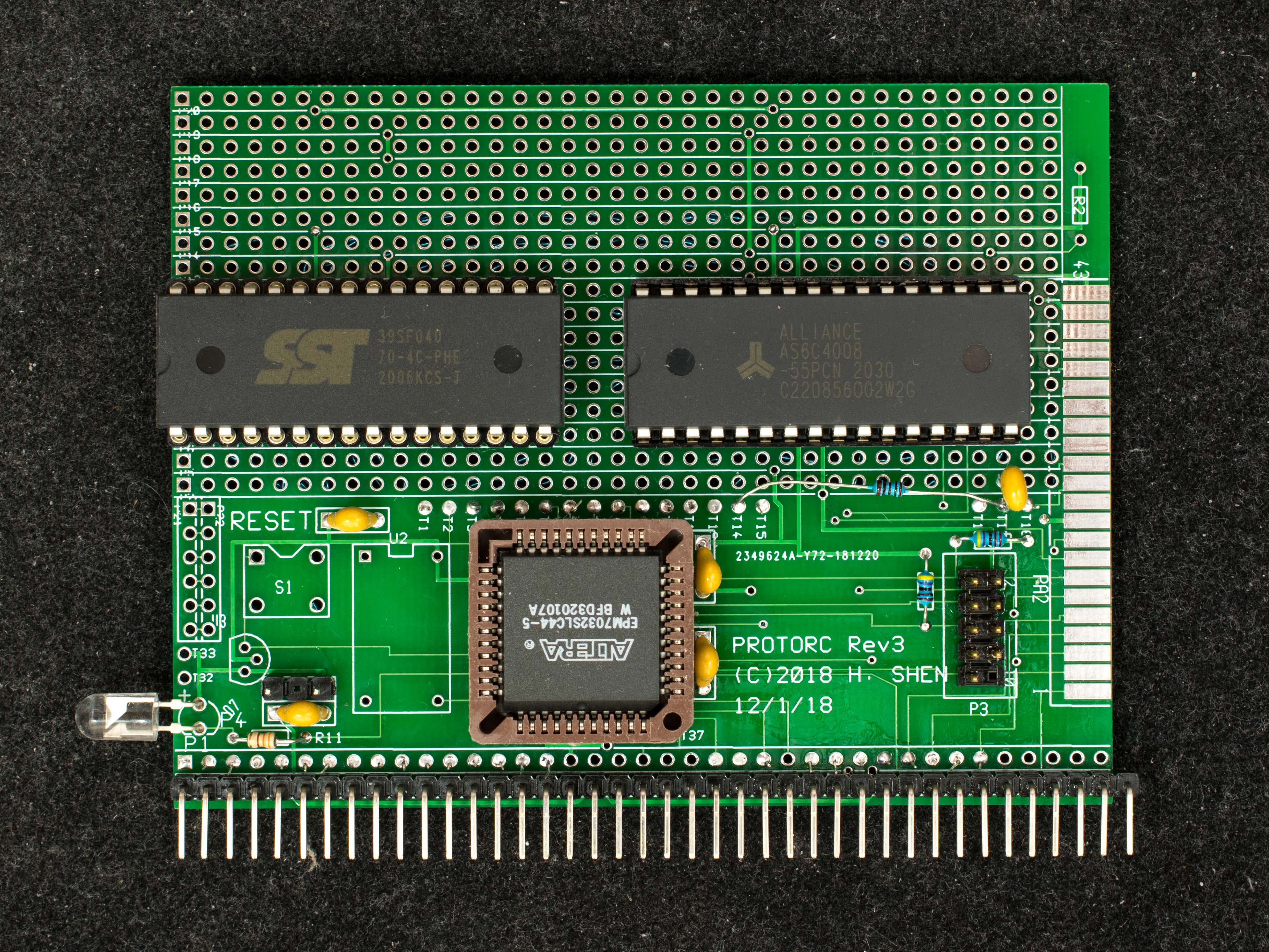
It's alive!
This is the logic portion of Wesley Isacks' schematic ported to Altera Quartus schematic. I drew the schematic using the same TTL devices (74138, 74174, 74257) from the Altera component library. The design compiled OK and used 50% of CPLD resource.
For the EPROM binary, I downloaded the RCZ80_pd1024.rom from Wesley Isacks' Github page, (https://github.com/PickledDog/rc-1024k/tree/main/firmware) and programmed ST39SF040 on my TL866 programmer.
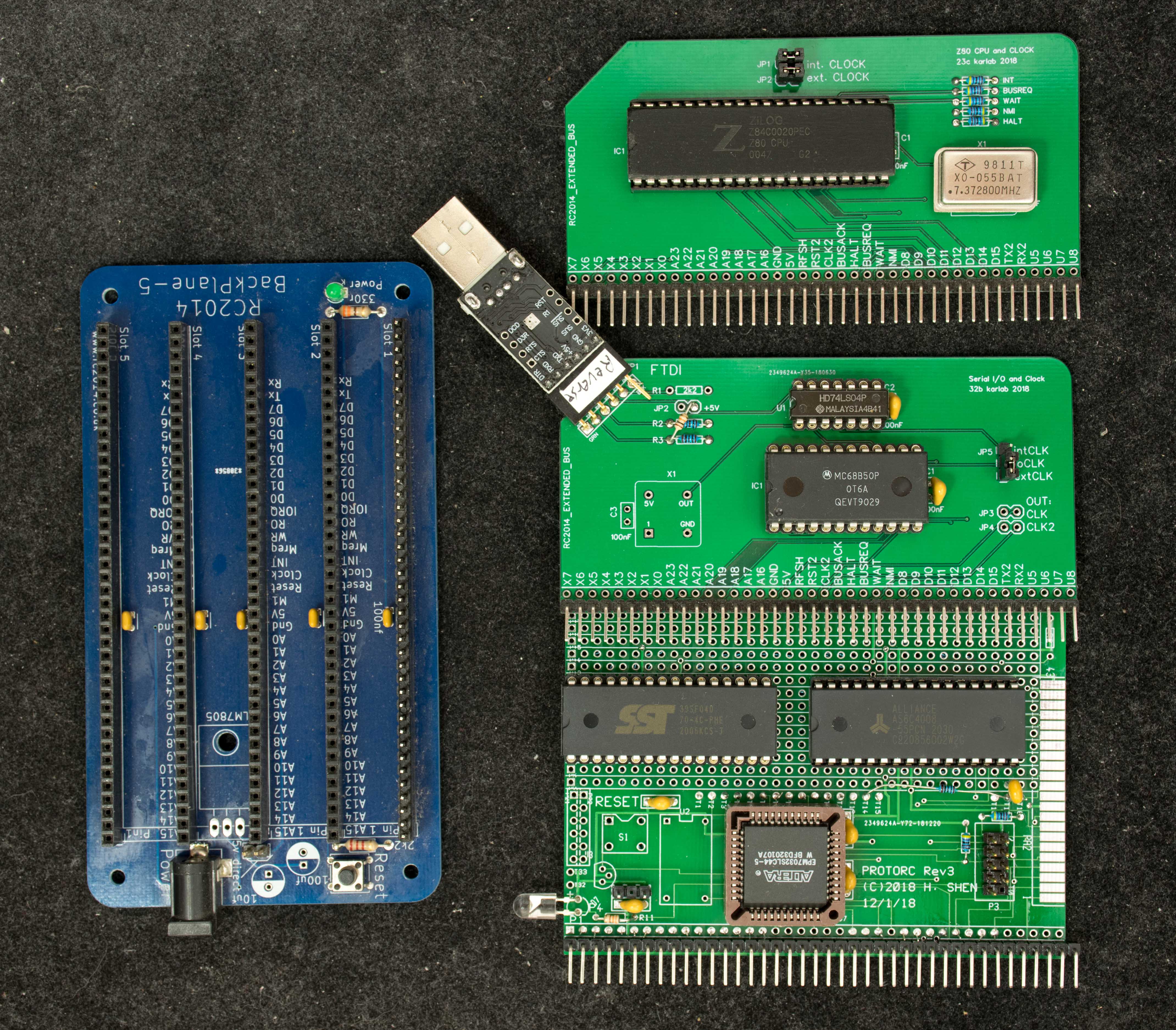
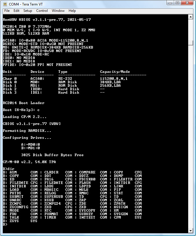
My setup is a 5-slot RC2014 backplane with Karlab #23c as Z80 with 7.37mhz oscillator, Karlab #32b ACIA, and Frugal RR512K.
Power up and it is alive!
Now, I'm going back to CPLD design to add a CF interface and possibly an I2C interface.
Bill
This is the logic portion of Wesley Isacks' schematic ported to Altera Quartus schematic. I drew the schematic using the same TTL devices (74138, 74174, 74257) from the Altera component library. The design compiled OK and used 50% of CPLD resource.
For the EPROM binary, I downloaded the RCZ80_pd1024.rom from Wesley Isacks' Github page, (https://github.com/PickledDog/rc-1024k/tree/main/firmware) and programmed ST39SF040 on my TL866 programmer.
My setup is a 5-slot RC2014 backplane with Karlab #23c as Z80 with 7.37mhz oscillator, Karlab #32b ACIA, and Frugal RR512K.
Power up and it is alive!
Now, I'm going back to CPLD design to add a CF interface and possibly an I2C interface.
Bill
On Friday, May 14, 2021 at 4:32:28 PM UTC-6 Bill Shen wrote:

Mark T
May 16, 2021, 9:27:37 PM5/16/21
to RC2014-Z80
Can you try the mods I described to see if that will then allow it to run the standard release of RomWBW?

Wesley Isacks
May 17, 2021, 2:34:28 AM5/17/21
to RC2014-Z80
Impressive stuff! Looks like this is coming along really nicely. Two thumbs up!
-Wesley
Bill Shen
May 17, 2021, 3:57:15 PM5/17/21
to RC2014-Z80
Mark,
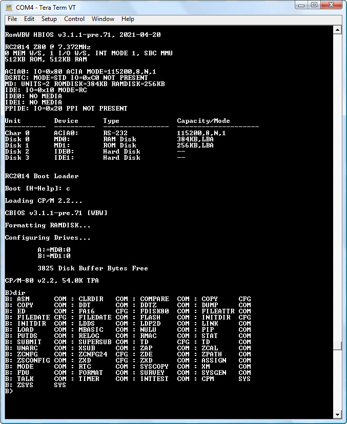
Yes, standard ROMWBW (pick "RCZ80 std" option when run buildrom script) works when the board is modified as you suggested:
---------------------------------------------------------------------------------------------------
I think the mods to make it compatible with RomWBW would be:
A1 to ‘138 pin 5 instead of A7.
D1 to ‘174 pin 3 instead of D0
D2 to ‘174 pin 4 instead of D1
D3 to ‘174 pin 6 instead of D2
D4 to ‘174 pin 11 instead of D3
D5 to ‘174 pin 14 instead of D7
----------------------------------------------------------------------------------------------------
Bill Shen
May 17, 2021, 4:09:18 PM5/17/21
to RC2014-Z80
Wesley,
Thanks.
SPLD and CPLD were developed in 1980's and 1990's, respectively to replace TTL logic. The golden era of CPLD was 1990's but then further IC integration had made CPLD obsolete. Atmel's ATF150x is about the only stocked CPLD devices now, but its design tool is downright awful. I design in Altera Quartus tool to program the (obsoleted) EPM7xxx CPLD or alternatively, use Atmel's translation tool to translate the design file to Atmel's programming format to program ATF150x CPLD.
Bill
Mark T
May 17, 2021, 4:49:55 PM5/17/21
to RC2014-Z80
Thanks for checking that Bill, I may try an SBC using simple TTL, though it looks like the flash is getting very hard to find in DIP32 so might need to use PLCC.
Bill Shen
May 17, 2021, 5:40:45 PM5/17/21
to RC2014-Z80
CF Disk
Since the addresses and data of CF interface on the prototype board is already wired, it is a matter of adding CF I/O addresses of 0x10-0x17 in CPLD and wire CF chipselect, CF read, and CF write control signals to the CF interface. CPLD logic utilization is now 53%.
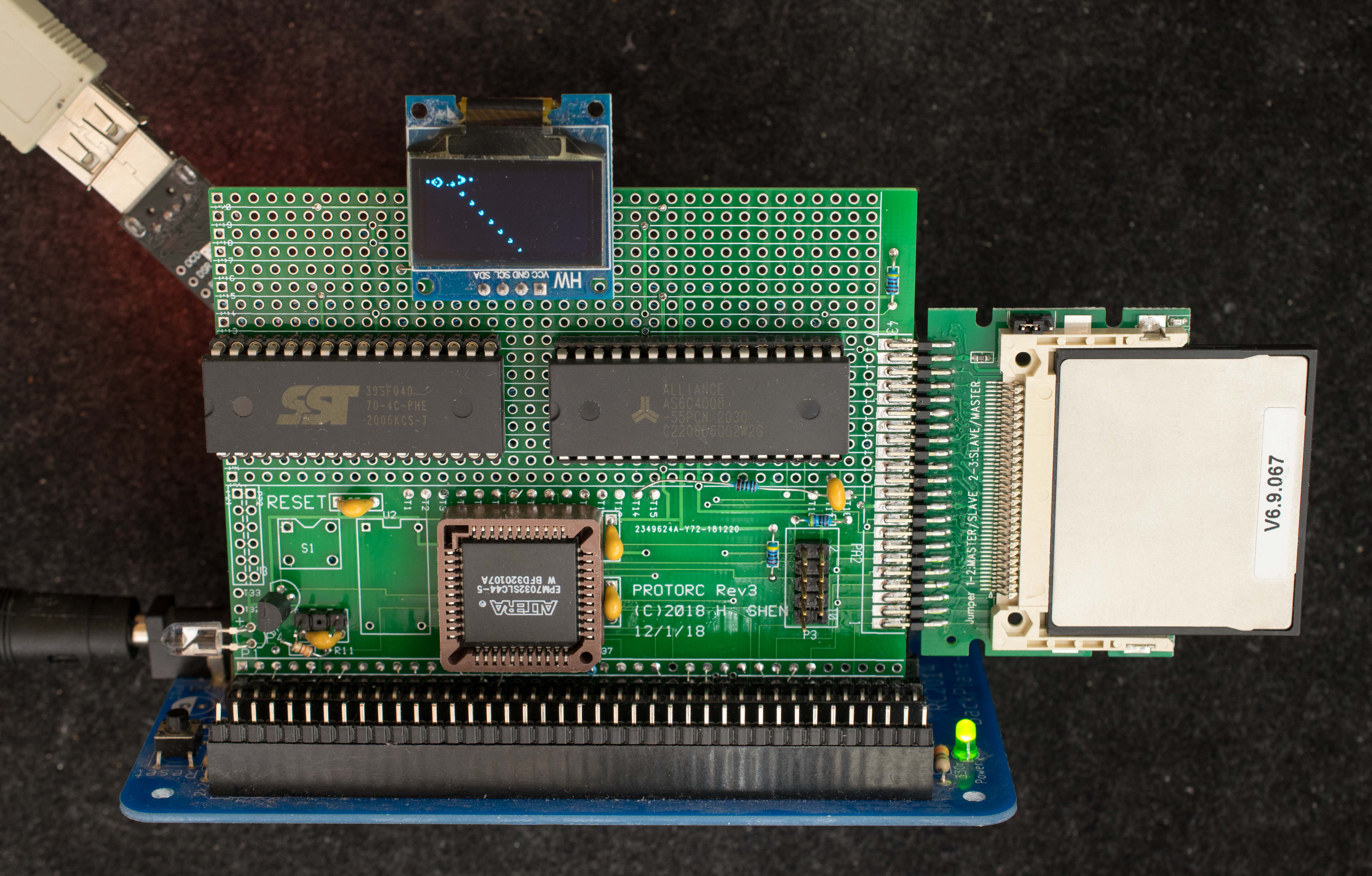
Attached picture show the installed CF interface.
ROMWBW autodetects the presence of CF disk and adds 8 slices to drives.
Only 53% of CPLD logic are used so it should be possible to build a 8-bit shift register to send a byte of data over I2C bus.
Bill
Since the addresses and data of CF interface on the prototype board is already wired, it is a matter of adding CF I/O addresses of 0x10-0x17 in CPLD and wire CF chipselect, CF read, and CF write control signals to the CF interface. CPLD logic utilization is now 53%.
Attached picture show the installed CF interface.
ROMWBW autodetects the presence of CF disk and adds 8 slices to drives.
Only 53% of CPLD logic are used so it should be possible to build a 8-bit shift register to send a byte of data over I2C bus.
Bill
On Friday, May 14, 2021 at 4:32:28 PM UTC-6 Bill Shen wrote:

karlab
May 17, 2021, 5:51:53 PM5/17/21
to RC2014-Z80
Hi Bill
You are taking the challenge very seriously and showing some quick result.
With your setup/breadboard you can jump into any problem/challenge without failing :)
Maybe you can diversify you project into one memory module (paged and linear memory) and a compact flash storage module with ic2?
Keep up the good work
Karl

Wayne Warthen
May 17, 2021, 5:57:42 PM5/17/21
to RC2014-Z80
This is really nice work Bill. A ton of functionality in a very cost effective package.
-Wayne
Wesley Isacks
May 17, 2021, 7:34:12 PM5/17/21
to RC2014-Z80
I've looked at CPLDs before, but didn't really know where to start. Terrible tools seems to be a recurring theme in this space... I will check out Quartus.
SPLDs I know (I program these in GALasm). I did try working a ATF16V8 into my board when I was designing it, but I couldn't seem to replace more than 2 chips with it.
-Wesley

Sergey Kiselev
May 18, 2021, 11:52:35 AM5/18/21
to RC2014-Z80
Wesley,
I used Quartus to design CPLD code / fuse maps. It is really flexible: You can do schematic capture - just using logic gates and connecting them together, or VHDL and Verilog among other things.
To program Atmel ATF150x series CPLDs, convert Quartus generated POF file to JED file using POF2JED tool provided by Atmel, and then use ATMISP tool, also provided by Atmel, to program the JED into the CPLD.
You are going to need a JTAG adapter. Unfortunately in case of CPLD they seem to be manufacturer-specific, and a bit expensive.
Atmel CPLDs use this: https://www.mouser.com/ProductDetail/556-ATDH1150USB
Altera CPLDs use this: https://www.mouser.com/ProductDetail/993-P0302 (cheaper clones with variable degree of compatibility are available elsewhere, google "USB Blaster")
It also might be possible to setup OpenOCD and use cheap FTDR232R based cable... but I haven't tried that just yet (https://www.hackup.net/2020/01/erasing-and-programming-the-atf1504-cpld/)
Thanks,
Sergey

Benjamin Scherrey
May 18, 2021, 1:03:04 PM5/18/21
to rc201...@googlegroups.com
Great stuff! An interesting side area from FPGAs that I've been curious about but never had a chance to check into.
- - Ben Scherrey
--
You received this message because you are subscribed to the Google Groups "RC2014-Z80" group.
To unsubscribe from this group and stop receiving emails from it, send an email to rc2014-z80+...@googlegroups.com.
To view this discussion on the web, visit https://groups.google.com/d/msgid/rc2014-z80/a52935ed-1751-429b-94a4-645fc5055036n%40googlegroups.com.
Bill Shen
May 18, 2021, 4:57:36 PM5/18/21
to RC2014-Z80
I2C Interface
Well, the wishful byte-write I2C capability is a bust because I ran out of I/O pins. There are only two I/O pins left after CF interface is implemented. Only 5 data lines are hooked up whereas byte-write function requires all 8 data lines to be hooked up to the CPLD. So unless I abandon the CF interface, which I'm not willing to do, the I2C function is limited to bit-by-bit data transfer, i.e., a bit bang I2C interface. Attached CPLD schematic shows the added CF interface and the bit-bang I2C interface. The logic is now 60% utilized but the I/O pins are 100% utilized.
The attached photo shows I2C interface added to the Frugal 512K RAM/ROM prototype board. A 128x64 OLED display is installed and the Game of Life, Gosper Glide Gun, is running over the I2C bus. It is rather slow, about 2 screen updates per second. Computation for each iteration of Life takes about 380mS and then it takes about 120mS to bit-bang the 1K bytes display data over I2C which translates to about 70K bit/sec, well short of the 400Kbit/sec capability of I2C. There are definite room for improvement. I have some ideas I want to try... There are certainly plenty of logic leftover to try some hare-brained ideas...
Bill
On Friday, May 14, 2021 at 4:32:28 PM UTC-6 Bill Shen wrote:
Mark T
May 18, 2021, 6:16:48 PM5/18/21
to RC2014-Z80
I don’t think you need M1 if you have IORQ and both RD and WR.
I think MREQ could use inverted IORQ.
Maybe reset could be generated internally by counting clock cycles while no active RD or WR. This would cost logic but save one pin.
Sergey Kiselev
May 18, 2021, 7:06:29 PM5/18/21
to RC2014-Z80
If I recall correctly, the M1 signal is used to distinguish between I/O and interrupt acknowledge cycles. It will be active (low) together with IORQ during interrupt acknowledge cycles, so that the interrupt controller can feed the interrupt vector / instructions (RST/CALL) to the CPU.
Mark T
May 18, 2021, 8:34:19 PM5/18/21
to RC2014-Z80
Yes but if you qualify IORQ with WR, or IORQ with RD, there is no need to disqualify with M1.
It can be useful to disqualify IORQ with M1, if using a ‘138 with IORQ and WR to decode both input and output operations, though you need to be careful with timing and direction of data on the bus.

Alan Cox
May 19, 2021, 6:41:15 AM5/19/21
to rc201...@googlegroups.com
On Wed, 19 May 2021 at 01:34, Mark T <mark...@gmail.com> wrote:
Yes but if you qualify IORQ with WR, or IORQ with RD, there is no need to disqualify with M1.It can be useful to disqualify IORQ with M1, if using a ‘138 with IORQ and WR to decode both input and output operations, though you need to be careful with timing and direction of data on the bus.
On the non Z80 cards I have M1 pulled high and mostly generate IORQ as !MREQ. If you are not using IM2 interrupts on the device it all seems to work fine. DRAM refresh and IM2 are the two interesting cases, but neither are being used.
5 data bits ought to be enough to do faster i2c - just do 0XXXX to load the upper half of the shift register and 1XXXX to load and fire, then read it back in nybbles. Z80 is actually not too bad at nibbles as rra is fairly fast and you can rotate one byte into pieces whilst the hardware sends the previous one. For block transfers in nibbles you've got the wonderfully obscure RLD and RRD. You can also have your I2C register over 8 addresses supplying the upper 3 bits although that might actually work out slower than 2 nybble writes. If you double buffer the 0XXXX it ought to be almost as fast as byte I/O without a FIFO in fact 8)
If there are spare pins an interval timer might be another thing to add - just needs an IRQ and a way to read and reset the bit indicating it is up. Ditto the rather nifty bitbang transmit/ byte buffered UART on your other CPU card but with a nybble sized CPU interface.
Alan
Bill Shen
May 19, 2021, 9:41:29 AM5/19/21
to RC2014-Z80
My thought on I2C bit banging is similar to why I've decided to bitbang the asynchronous serial transmit at 115200: at high serial speed, Z80's interrupt overhead makes serving serial port with interrupt inefficient, so it is better just poll the serial flags; but if the CPU is spinning on the flag waiting, it might as well rolling up its sleeve and do the actual work of banging out data one bit at a time.
This is a good opportunity of thinking about various ways of bit bang (or nibble-bang) I2C. If CPLD is low on logic, I can hook up A0 to input of SCL flipflop instead of D0 so even I/O address (SCL0) drives SCL low and odd I/O address (SCL1) drives SCL high. This way, this 4-instruction loop will bang out a bit of data:
out (SCL0),a ;output d7 on SDA while SCL low
out (SCL1),a ;output d7 on SDA while SCL high
out (SCL0),a ;SCL return to low
rla ;next bit
... do this 7 more times
At 7.37MHz this routine bitbang data out about 200Kbit/S
If CPLD has more logic resources, then a self-clocking SCL can speed up the bitbang routine: writing to a self-clocking I/O address causes a counter to count up so at count 4 (0.5uS) SCL goes high and at count 15 (2uS) SCL returns to low. This way the software only needs to write data to the self-clocking address, shift data left, and repeat. This is capable of 400Kbit/S.
Good thing about designing with CPLD is I can put off the specific hardware implementation and move forward to PC board layout. I'm going to start a new thread regarding the PC board layout because I'm planning on something completely different...
Teaser: the title of the new thread is "Universal I/O board for RC2014"
Bill
Alan Cox
May 19, 2021, 11:46:56 AM5/19/21
to rc201...@googlegroups.com
On Wed, 19 May 2021 at 14:41, Bill Shen <coinst...@gmail.com> wrote:
My thought on I2C bit banging is similar to why I've decided to bitbang the asynchronous serial transmit at 115200: at high serial speed, Z80's interrupt overhead makes serving serial port with interrupt inefficient, so it is better just poll the serial flags; but if the CPU is spinning on the flag waiting, it might as well rolling up its sleeve and do the actual work of banging out data one bit at a time.
Totally agreed - I was very dubious when I first saw it but the timing and performance of it versus a basic non FIFO uart like the ACIA were the same on transmit. Interrupt for receive is high value for some use cases but at higher speeds the tx interrupt isn't a lot of use even on processors with much better interrupt performance.
If CPLD has more logic resources, then a self-clocking SCL can speed up the bitbang routine: writing to a self-clocking I/O address causes a counter to count up so at count 4 (0.5uS) SCL goes high and at count 15 (2uS) SCL returns to low. This way the software only needs to write data to the self-clocking address, shift data left, and repeat. This is capable of 400Kbit/S.
That's kind of how the bit bang SPI works on some of the other systems I've used - the write of the bit triggers the clocking. The only difference being that with SPI because the link is bidirectional you drive the output with an in () statement. A0 is the bit to clock out, D0 is the last bit received. (rr c rla rl c in a,(c) rla rl l).
Alan
Reply all
Reply to author
Forward
0 new messages