Front panel board for RC2014
494 views
Skip to first unread message

Bill Shen
Dec 23, 2022, 8:46:29 AM12/23/22
to RC2014-Z80
The current discussion about front panel and Hackday's article reminded me of my experience with Altair 8800 front panel many decades ago. The panel of lights and switches were fun to look at but decoding the binary LED patterns and manually toggled in data were not very practical then nor now. I do like the opportunity of entering code right after system reset, but the process should be more user-friendly. By "more user-friendly" I'm thinking about 7-segment display for 16-bit addresses and 8-bit data; and instead of toggling each bit with a switch, I thinking of data entry with a PS2 keyboard.
The early front panels were implemented with discrete TTL logic but re-do the front panel with programmable logic is easier and better fit for the more limited space on RC2014 backplane.
I may want to build a dedicated front panel board later, but I want to utilize boards I have on hand to exploring the concept . Here are two RC2014-compatible boards that may be applicable;
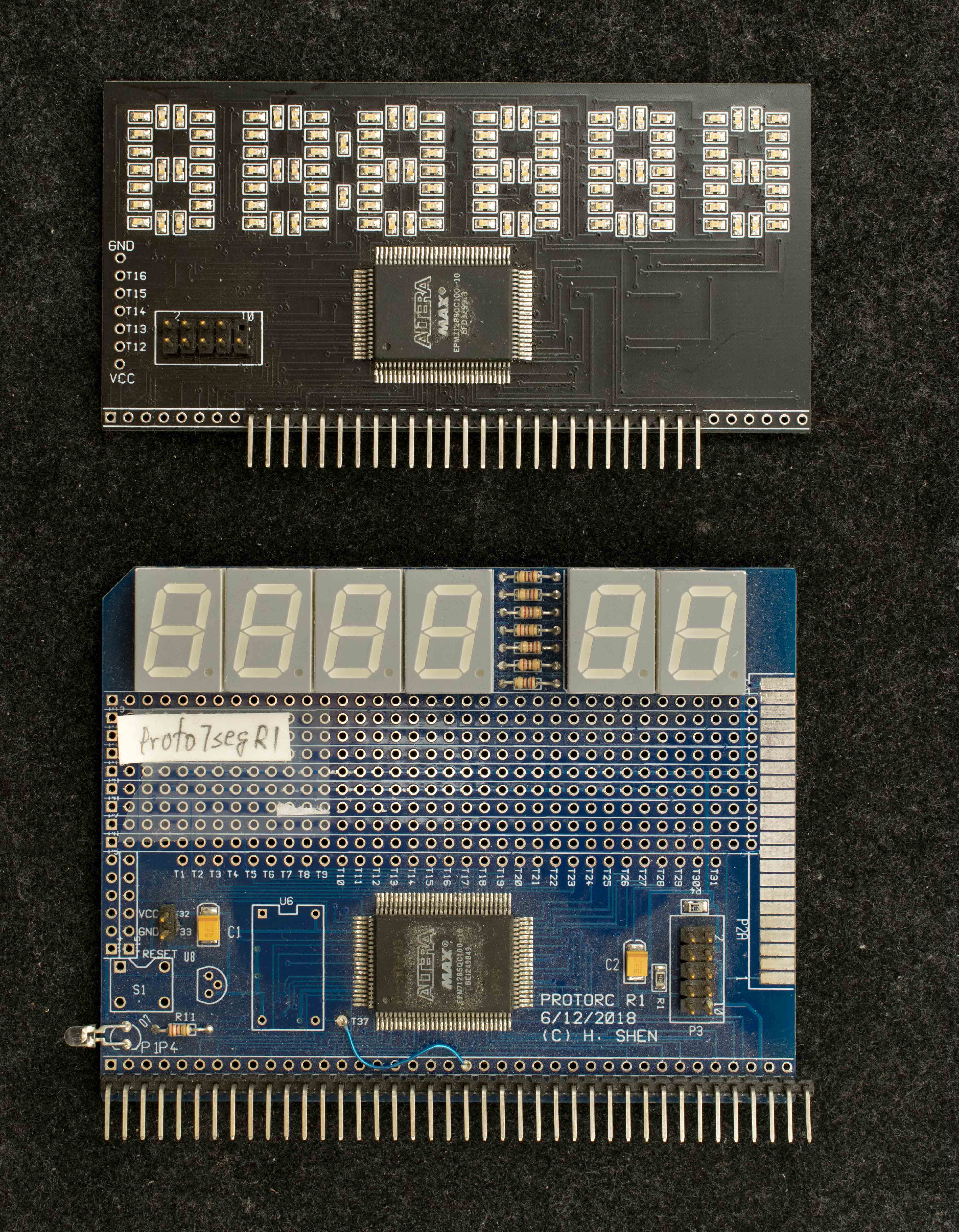
The top display board with discrete LEDs is in standard RC2014 dimension (50x100mm). The LEDs are controlled by a EPM7128S CPLD at the back of the board. It has some spare pins at the left of the board for a PS2 keyboard. It looks good as the RC2014 front panel but so much of the CPLD resources are dedicated to driving the 122 LEDs, there may not be sufficient logic left.
The bottom board is a RC2014 CPLD proto board with six 7-seg displays. The CPLD logic is mostly available, there are plenty of spare pins and there is a prototype area for PS2 keyboard. I'll start the project with this board.
To be continued...
The early front panels were implemented with discrete TTL logic but re-do the front panel with programmable logic is easier and better fit for the more limited space on RC2014 backplane.
I may want to build a dedicated front panel board later, but I want to utilize boards I have on hand to exploring the concept . Here are two RC2014-compatible boards that may be applicable;
The top display board with discrete LEDs is in standard RC2014 dimension (50x100mm). The LEDs are controlled by a EPM7128S CPLD at the back of the board. It has some spare pins at the left of the board for a PS2 keyboard. It looks good as the RC2014 front panel but so much of the CPLD resources are dedicated to driving the 122 LEDs, there may not be sufficient logic left.
The bottom board is a RC2014 CPLD proto board with six 7-seg displays. The CPLD logic is mostly available, there are plenty of spare pins and there is a prototype area for PS2 keyboard. I'll start the project with this board.
To be continued...
Bill Shen
Dec 23, 2022, 8:53:51 AM12/23/22
to RC2014-Z80
Correction:
The CPLD controlling the 122 LEDs is in the front of the pc board. I was confused with many resistors and switching transistors at the back of the pc board.
Bill
The CPLD controlling the 122 LEDs is in the front of the pc board. I was confused with many resistors and switching transistors at the back of the pc board.
Bill

Tadeusz Pycio
Dec 23, 2022, 9:37:44 AM12/23/22
to RC2014-Z80
Hi Bill,
There is a project that is a reactivation of a Z80 trainer popular in Poland in the '80s called CA80, which used a hexadecimal keyboard and LED displays. https://github.com/ZegarNotAvailable/CA80-na-RC2014
Bill Shen
Dec 23, 2022, 11:02:41 AM12/23/22
to RC2014-Z80
Tadeusz,
It looks interesting. However, I think the keyboard and display are driven by RC2014 via 82C55 on CA80's SYS I/O board. Whereas keyboard/display and hardware of a front panel halt Z80 and take over RC2014 bus to display/modify memory and single step Z80.
Bill
It looks interesting. However, I think the keyboard and display are driven by RC2014 via 82C55 on CA80's SYS I/O board. Whereas keyboard/display and hardware of a front panel halt Z80 and take over RC2014 bus to display/modify memory and single step Z80.
Bill
Bill Shen
Dec 23, 2022, 11:11:47 AM12/23/22
to RC2014-Z80
My front panel concept was first implemented on the CPLD trainer but not very well documented. RC2014 is a different computer so the design will be different and this is a good opportunity to document it better.
Theory of Operation
The front panel has two modes of operation, data entry mode and run mode. In data entry mode Z80 BUSREQ is asserted so Z80 address/data/control signals are tri-stated and CPLD is controlling the bus. The CPLD listens to PS2 keyboard and drive the 7-seg display according to the keyboard commands. The decimal points of all 7-seg display are lit when in data entry mode. There are just a few keyboard data entry commands to show or modify memory:
'Space', 'Enter', 'Backspace' are the only ways to change memory's address field:
* 'Space' key reset address value to 0x0
* 'Enter' key writes displayed data to current memory location, then reads and displays content of next memory location
* 'Backspace' key decreases current memory location by one, then reads and displays the memory content.
Keys 0-9, a, b, c, d, e, f are hexadecimal input for the 8-bit data field. Following a 'Enter' keystroke, a hexadecimal key input will modify the most significant nibble; next hexadecimal key input will modify the least significant nibble; if there are additional hex input, the active digit will alternate between the most significant and least significant digit.
'Escape' key toggles between data entry mode or run mode.
BUSREQ is negated when in run mode. Z80's WAIT signal is used to single step or run continuously. The 7-seg display shows the current address generated by the Z80 processor and data read or written by Z80. The run mode only has two commands:
* 'S' key to single step, Z80 steps one instruction with every 'S' key pressed.
* 'R' key to toggle between Run and Single-step.
That's the concept for now. No processor is involved, everything will be implemented in CPLD state machines. I'm sure I'll make up more stories as I go along!
Bill
On Friday, December 23, 2022 at 6:46:29 AM UTC-7 Bill Shen wrote:

Sławomir Zegarliński
Dec 23, 2022, 11:44:59 AM12/23/22
to RC2014-Z80
Hi Bill.
The CA80 has all the features you are talking about. The monitor is written in such a way that the user has the impression that he is using two computers at the same time: a supervisor and a user. The supervisor can execute the user's program in stepping or with traps. After each step you can view - modify registers, memory and I/O. Everything fits in 2 KB of ROM. The display and hexadecimal keyboard are handled in NMI every 2ms. One Z80 takes care of everything. :-)

Mark T
Dec 23, 2022, 12:25:38 PM12/23/22
to RC2014-Z80
Both the CA80 and the CPLD method require programmed devices. Although the Altair type of panel was quite clumsy it did provide a way to bootstrap without a programmer. With battery backed ram and a write protect switch you can avoid reloading the bootstrap unless you make any hardware changes affecting the ram. Using the scrumpi method with single step circuit and the processor generating the address the component count can be reduced and create a system that can be bootstrapped without a programmer. FT245 can also be used in a similar way to avoid the tedious switches, though using switches and single step circuit can often help diagnose a faulty system using only a logic probe or multimeter.
Bill Shen
Dec 23, 2022, 1:56:04 PM12/23/22
to RC2014-Z80
There are lots to be said for software monitor that can single step, set breakpoint, display processor registers/status--this is probably why there are not many hardware-based debugger or front panel control. My original thought was since I already have 7-segment LEDs for display and programmable logic device for its control, it may be possible to use PS2 keyboard to input small program into memory and monitor/control every step of Z80 operation starting from reset.
But what I heard so far is there isn't much interests in hardware-based single stepper and debugger/monitor. I get that, actually, front panel is mostly "Hollywood" but of limited utility even with the original Altair computers even though these early computers are memorable because of their front panels.
Well, at least I didn't have to do all these works shown in Hackaday's article.
Bill

Le Fauve
Dec 26, 2022, 8:19:24 PM12/26/22
to RC2014-Z80
Since we talk about front panels, I do have a question.
I've started to think about making one, not because it would be useful but because I think it's a good way to learn more about the inner working of the Z80.
I think displaying and/or editing RAM content should be "easy", but there is one feature I'd like to have which is a little less straight forward:
I would really like to be able to change the PC from the front panel.
From what I've read, the usual way to do this is to inject a "jump" command on the bus before sending the address bytes on the data bus, but unless I'm wrong, it means I'll have to find a way to deactivate the ROM and RAM's CS when the Z80 will try to fetch the next instruction.
Also, I haven't find any reference about this being done in previous projects, but I'm thinking that since there is only 64KB or addressable memory, it may be easier to just inject "NOP"s on the data bus until the PC is at the desired value (that would be the new value minus one).
Even if the panel has to stop the Z80 after each instruction to check the current PC value, that should still be fast, and I'll be happy with reaction time of less than 0.5 seconds.
So, what I'd like to know is:
- Do I really need to disable the CS of RAM and ROM to allow instructions injection by the panel (or is it an easier way)?
- Has my "NOP" solution any chance to work? (When I get a "new" idea on a 40+ years old platform and I cannot find trace of anyone having had the same idea before, the most likely explanation is that this isn't a good idea, but I cannot see why at the moment :o) )
Cheers,
Eric
Mark T
Dec 26, 2022, 11:55:48 PM12/26/22
to RC2014-Z80
I can’t think of any reason why injecting NOP until the PC reaches the target address wouldn’t work.
The method I use is to write a jump to target into RAM at 0000, then single step the jump.
There are various ways to inject NOPs. As you already suggested by disabling the CS of ROM and RAM. You could also disable MREQ or RD from the Z80, or disable a data bus buffer between the Z80 and the memory. There is also the method used by the old Zx80/81, 1k resistors between the processor and memory and pull the databus on the z80 side down to 0v, not sure how well that would work at RC2014 clock speed.
Le Fauve
Dec 27, 2022, 2:29:10 AM12/27/22
to RC2014-Z80
Thanks Mark,
I'm using a "RC2014 classic" with no memory paging, so I cannot use your trick because my address 0000 is always ROM.
I'm trying to do as few as possible modifications to the RC2014 so adding a buffer
or resistors
between the RAM/ROM and the rest of the bus may be tricky.
What I was planning was to use one of the 4 unused signals of the bus as an "enable memory CS" signal, and somehow add an AND gate on both the ROM and RAM boards (hoping that I may find some unused gates on one of the chips already preset on those boards).
After reading your message, I'm considering modifying the CPU board to disable RD or MREQ instead, but wouldn't this cause timing issues if I add a gate to those signals?
Unless I just add a 1K resistor between the Z80's RD (or MREQ) and the bus? This way, if the panel raises the line to VCC, neither the RAM nor the ROM should be selected? (this would have the bonus to keep the RC2014 working when the panel isn't plugged in the bus, as well as not using any extra line on the bus)
I'm honestly ways above my comfort level here :o) This is really interesting, but I would really like not frying anything :o)
Eric
Bill Shen
Dec 27, 2022, 10:21:16 AM12/27/22
to RC2014-Z80
Looking over RC2014 Classic schematic, I see the RAM. board has A15 inverted as RAM’s chip select. So you can remove the 7404 inverter, jumper the inverter’s input pin to output pin and thus move RAM’s memory map to 0-$7FFF. You can then remove the ROM board and have the front panel initialize RAM and boot Z80 from RAM.
Bill
Mark T
Dec 27, 2022, 10:29:49 AM12/27/22
to RC2014-Z80
Hi Eric,
It might be easier to keep most of the mods on the backplane. If you have the eight slot backplane you could use slot 1 for your panel, slot 2 for cpu, and cut the RD track between slot 2 and 3, then link from an unused pin on slot 1 from your front panel board to RD on slot 3.
The eight slot backplane also provides options for resistors in the data and address lines between slot 2 and 3, so you could try the resistors to isolate the data bus, but I think adding control to RD is simpler.
The front panel probably needs some support if you mount it vertical with the other modules, but you could mount it flat above the backplane with spacers to keep it stable.
If you are going to use point to point wiring on breadboard you could build in stages and test each part as you progress. I’d suggest starting with a single step circuit, then maybe a display for data and address.
the single step circuit I used might be usefull as a starting point
Mark
Le Fauve
Dec 28, 2022, 7:44:27 PM12/28/22
to RC2014-Z80
Thanks for the feedback!
Bill, I didn't thought about removing the ROM board. That would work, but I would like to still be able to use the RC2014 with the SCM or BASIC so it may not be very convenient in my case to have to remove a board when I want to use the front panel.
Mark, I didn't consider using the isolated slots for this, but this is indeed the easier solution. I already put two rows of male pins headers between slots 6 and 7, and I'm using jumpers to connect the signals.
It's a little tight (the bottom of card in slot 6 touch the top of the jumpers) but it does work and I can probably do the same between 2 and 3.
I didn't do it at the same time I added the 6/7 headers because I wanted to be able to add resistors if needed (for the CF card board, I think that was recommended) but I don't think I'll go this road (I love the "micro 8 bits experience" and I have other things running CP/M).
For the mechanical side of things, I ordered some short IDE ribbon and I was thinking to have a very short board bridging the bus to a 40 pins IDE connector and connect the panel to it, so it can be mounted on the outside case when I'll make one. That will also make it easier to test things on a breadboard.
Hopefully the 10cm cable wont add too much interference.
Thanks for your schematics. My first step will probably be to implement a "run/halt" switch using BUSRQ, but single step will probably be the next thing.
I was planning to use some 74HC74 flipflops I have around for the debouncing, but I'll look at your schematic for ideas (I had a quick look but it's a little complex for me at the moment).
Also it seems you just use resistors and led to connect the leds to the address bus. Isn't this risky? I was planning to use74LS274 buffers between the bus ans the leds.
Cheers,
Eric
Mark T
Dec 29, 2022, 11:06:30 AM12/29/22
to RC2014-Z80
Hi Eric,
There is also the option to put the header pins for links on the under side of the backplane if you put spacers as feet on the backplane.
0603 smt resistors fit quite nice between pin header pads so you could put 1k or 2k resistors in series with the data pins and fit a link when you want to bypass the resistor.
You could use 74hc74 as set/reset latch for debouncing switches, but you can also use any non-inverting HC(T) gate as a set/reset latch by adding a 10k resistor from the output to the input. Pull the input high to set and pull it low to reset. You could use an SPDT switch to debounce the switch, or use two separate tactile switches. If you use two separate tactile switches put a 1k series resistor in the pullup to avoid shorting out the supply. 74HCT245 could debounce eight inputs.
You probably don’t need to debounce switches for setting the data and address inputs, typically only clock inputs need to be debounced.
I have another board with a single step circuit using the 74LS123 that might be easier to understand. I’ll dig out the schematic next time I boot up the laptop. It also provides a single cycle option to pause on each read or write cycle of each instruction, which can be interesting to understand the z80 bus interface. Unfortunately it doesn’t pause on refresh cycles or the initial state of interupt cycle as the z80 does not wait on these cycles.
Manual clocking the z80 is another interesting excercise, using a debounced toggle switch to set the clock high or low.
I’m not sure how usefull setting busreq will be unless you have something else take control. Note that after reset the z80 will still fetch the first instruction before it acknowledges the busreq.
Mark
Mark T
Dec 30, 2022, 7:59:11 PM12/30/22
to RC2014-Z80
Attached single stepper circuit schematic. This will stop at each bus cycle that supports wait or can be set to stop only on the next M1 fetch in which case it pauses 0.3 seconds at each bus cycle so you can still see the read and write operations as they progress. It also decodes the control signals to indicate memory read, memory write, input, output etc.
Unfortunately this version only works if the z80 clock is greater than 18 MHz as it reasserts wait too soon for slower clock frequencies and the z80 can not continue. It might be possible to make it work using 74LS395 and adding some extra delays.
Bill Shen
Jan 1, 2023, 10:01:25 AM1/1/23
to RC2014-Z80
I added a PS2 connector the the display prototype board (connector at lower left of the photo) and 4 blinky lights mapped to low nibble of I/O address 0x0. Left four 7-seg display is for addresses and right two 7-seg display is for data.
These features are implemented in CPLD state machines:
* After reset Z80 is bus master in single step mode. Keyboard input 'S' single-step Z80; keyboard input 'R' toggles Z80 between continuous run or single step. Keyboard input 'Esc' asserts Z80 nBUSREQ and the front panel state machine takes over Z80 bus after current cycle is completed. 'Esc' toggles bus mastership between Z80 and Front Panel State Machine.
* When Front Panel State Machine is the bus master, keyboard input 'Space' set the address field to 0x0 and read/display memory value of 0x0; keyboard input 'Enter' writes displayed data value to current address location, advances address by 1, then display the memory content of address+1; keyboard input 'Backspace' decreases address by one then display the memory content of address-1. Keyboard input '0' to '9', 'a' to 'f' changes the memory content of current address. Data value is not written to memory until 'Enter" is pressed
118 macrocells of the 128-macrocell CPLD are utilized (92% utilization) for the Front Panel State Machine. I added 4 discrete LED output at I/O address 0x0 as blinky lights. The design uses Z80's BUSREQ and WAIT signals which are available in Enhanced RC2014 bus. The prototype board has the standard RC2014 bus so BUSREQ and WAIT are wired to two of the 4 SPARE pins
This design lacks a couple features:
1. Ability to read/write memory at arbitrary address location while Front Panel State Machine is the bus master. 'Space', 'Enter', and 'Backspace' keys are only way to change address values; it would be nice to enter arbitrary address value via keyboard.
2. Ability to change Z80's Program Counter while Z80 is the bus master. Right now Z80 reset forces PC to 0x0 and it should be fairly easy to force PC to 0x66 using NMI but it would be nice to force Z80 to jump to user specified address.
For feature item 1 I may be able to added another keyboard command to transfer displayed data to displayed address field, but for feature item 2 I'm at lost about how to force jump instruction and associated addresses into Z80.
Bill
On Friday, December 23, 2022 at 6:46:29 AM UTC-7 Bill Shen wrote:
Mark T
Jan 2, 2023, 12:10:31 PM1/2/23
to RC2014-Z80
Hi Eric,
I forgot to reply on the LEDs. These are direct off the address bus but the address bus is only driven by the 74hct245 buffers which have more than enough drive capability to drive the address bus and the LEDs. Also using green LEDs the LEDs don’t start to draw any current until after the address line is already above the ttl logic 1 threshold. I also disable the LEDs when not in step mode.
The data bus LEDs are only driven when reading from data bus, so again driven by the 74hct245 and disabled when not in step mode.
I probably wouldn’t use the same method to inject NOP if I respin the board.
Mark
Bill Shen
Jan 2, 2023, 8:26:25 PM1/2/23
to RC2014-Z80
I overhauled the address generation logic to have the ability to enter arbitrary address so now I can easily read and modify any memory location when Front Panel is the bus master. The command I added is 'X' that redirects next 4 keystrokes to edit the 4-digit address field. The CPLD resource is now 100% utilized so these are all the features I can have for this CPLD. In any case, I can't figure out how to change Z80's PC unless I'm willing to jam CPLD's output in collision with RAM/ROM data bus. CPLD is actually strong enough to overpower RAM/ROM but intentionally creating data contention is just not cool.
For completeness, the CPLD schematic is attached; it is chaotic and complicated so I'm not prepared to explain it unless people really want to know. The front panel works well, I can enter 50-byte or so program pretty quickly from PS2 keyboard and run/single-step the program. Operation of the front panel is hard to visualize so I plan to make a couple videos showing how the front panel controls SC108+ACIA or a RC2014Pro-look-alike.
Bill
Le Fauve
Jan 6, 2023, 6:54:42 AM1/6/23
to RC2014-Z80
Mark, thank you again for all those information.
>
There is also the option to put the header pins for links on the under
side of the backplane if you put spacers as feet on the backplane.
I do have spacers, but I don't like to have to turn the whole RC2014 upside down whenever I want to add or remove a jumper :o)
I did consider inserting the pins from the underside, though, in order to save 1 or 2mm that should be enough to resolve the problem, but I just realized that because the "RC2014 Classic" boards aren't all inserted in the same orientation (for some you see the components side, for others you see their backside) I won't have the same issue I had between slots 6 and 7 (the CPU board that will be in slot 2 will be away from the pins). I will just do the same thing I did for the other pin headers.
>
0603 smt resistors fit quite nice between pin header pads so you could
put 1k or 2k resistors in series with the data pins and fit a link when
you want to bypass the resistor.
I did consider this at some point, but that wouldn't allow me to totally isolate a line so I didn't (but doing it only for the data bus probably won't be an issue though; I'll keep the idea in case I eventually need resistors on some pins)
>
You could use 74hc74 as set/reset latch for debouncing switches, but you
can also use any non-inverting HC(T) gate as a set/reset latch by
adding a 10k resistor from
> the output to the input. Pull the input high
to set and pull it low to reset. You could use an SPDT switch to
debounce the switch, or use two separate tactile switches. If
> you use
two separate tactile switches put a 1k series resistor in the pullup to
avoid shorting out the supply. 74HCT245 could debounce eight inputs.
I will definitely try those methods (I like the one with the 74HCT245, because iiuc that should give me more than enough debounced inputs with only one chip and a few resistors :o)
>
You probably don’t need to debounce switches for setting the data and
address inputs, typically only clock inputs need to be debounced.
Yes, I was planning to only debounce halt/run and step; I may need to also debounce "Examine next" and "Deposit next" if I end up having those (they seem convenient to edit or examine many bytes in a row).
>
I have another board with a single step circuit using the 74LS123 that might be easier to understand.
Thanks a lot, I can definitely use some inspiration (did I mention I never did anything so advanced before :o) ?)
>
Manual clocking the z80 is another interesting excercise, using a debounced toggle switch to set the clock high or low.
I like the idea, but that may be something I'll add later, when basic features are working.
> I’m not sure how usefull setting busreq will be unless you have
something else take control. Note that after reset the z80 will still
fetch the first instruction before it acknowledges the busreq.
The idea is that whenever the panel puts the RC2014 in "Halt" mode, the panel can be used to read/write memory. Using busreq to pause (going in "Halt" mode) makes it automatically the case.
I will have to find a way to prevent those features to work when in Run mode (perhaps by just using the busack as a prerequisite? I didn't think all the details yet).
> I forgot to reply on the LEDs. These are direct off the address bus
but the address bus is only driven by the 74hct245 buffers which have
more than enough drive capability to drive
> the address bus and the LEDs.
Also using green LEDs the LEDs don’t start to draw any current until
after the address line is already above the ttl logic 1 threshold. I
also disable
> the LEDs when not in step mode.
I was planning to use buffers which are always latched so the leds always show the value of each bit of the bus. The buffer will basically just be there to protect the rest of the bus.
I didn't realized the color of the leds could have an effect though.
Having read all this, I'm wondering if my first step shouldn't be to just display the data, address and some control lines state with leds, and to try clocking the Z80 by hand as you recommended.
Just to have an easier way to understand what's happening, before starting working on the actual panel.
Bill, your panel looks great!
I apologize for having kind of hijacked your thread. I didn't thought my initial questions will get so much answers (not that I'm complaining :o) Thanks again guys! ).
I'll try to create a new thread whenever I'll have more specific questions (it will take me some time to digest all the information I got from this one ;o) ).
Cheers,
Eric
Reply all
Reply to author
Forward
0 new messages