Hello / my Z180 computer project
1,466 views
Skip to first unread message

Alastair Patrick
Jan 4, 2022, 8:14:25 PM1/4/22
to retro-comp
Hi,
I'm planning a homebrew computer as a hobby project. These are the tentative features:
- All parts available new for sale, i.e. no salvaged parts
- Through-hole parts
- Z180 CPU with 2x on-chip UARTs
- 512K static RAM
- 512K flash ROM with RomWBW installed
- PS/2 keyboard using 1 integrated UART
- RS232 using the other integrated UART and MAX232 for level shifting
- TMS9918 compatible video display controller with HDMI output
The main differentiating feature would be that the TMS9918 would actually be emulated using an FPGA. I don't think there are any 5V FPGAs. I found some 5V CPLDs but they do not have enough macrocells to implement a TMS9918. So to avoid voltage level shifting complications with the FPGA, I plan to use a single 3.3V supply for the whole computer. That means using a 3.3V CPU, which motivates a Z180 CPU rather than a Z80 CPU, since Z180 is available in 3.3V, while Z80 is not.
The FPGA would emulate not only the TMS9918 but also all the connected video DRAM, a scanline doubler and an HDMI video encoder, allowing connection to a modern TV. I would start with the TMS9918 VHDL source files from the MISTer project and adapt them. I've been looking at FPGA dev boards ranging in capability from the Pluto-IIx to the Mercury 2.
I am a professional software engineer with assembly language experience, starting with Z80 programming on the Sinclair ZX Spectrum 30+ years ago. In the late 90s and early 00s, I worked as a video games programmer, specializing in graphics programming, so have a software level understanding of hardware like the TMS9918. My electrical engineering experience is much more limited though. I did EE for my first two years in college before switching to SWE. The only thing I've done with an FPGA so far is have it blink an LED. I hope my programming skills will help me learn Verilog and VHDL and port the TMS9918 code from the MISTer project.
I'm not really looking for any specific advice. Mostly thought I'd say hello and give people who know much more than me an opportunity to point out if I'm making any obvious mistakes.
Maybe I'll ask, do you know of any other projects combining a real CPU with FPGA emulated TMS9918? If you wanted to design a computer incorporating both a Z80 and an FPGA, how would you address the incompatible supply voltages?
Al

Alan Cox
Jan 5, 2022, 9:44:45 AM1/5/22
to Alastair Patrick, retro-comp
On Wed, 5 Jan 2022 at 01:14, Alastair Patrick <alastai...@gmail.com> wrote:
Hi,
I'm planning a homebrew computer as a hobby project. These are the tentative features:
- All parts available new for sale, i.e. no salvaged parts
- Through-hole parts
- Z180 CPU with 2x on-chip UARTs
- 512K static RAM
- 512K flash ROM with RomWBW installed
- PS/2 keyboard using 1 integrated UART
I am not sure the Z180 UART can be persuaded to talk to a PS/2 keyboard. It isn't a standard serial protocol but a rather strange synchronous clocked interface. As you are using an FPGA there are tons of FPGA PS/2 keyboard interface designs you could use instead.
- RS232 using the other integrated UART and MAX232 for level shifting
- TMS9918 compatible video display controller with HDMI output
The main differentiating feature would be that the TMS9918 would actually be emulated using an FPGA. I don't think there are any 5V FPGAs. I found some 5V CPLDs but they do not have
There are a tiny number but they won't have enough macrocells. There is a direct link between voltage level and feature size on an IC, so as your feature size shrinks and the macrocell count goes up you are pretty much unavoidably driven down to 3.3, and then 1.8v for the big ones.
enough macrocells to implement a TMS9918. So to avoid voltage level shifting complications with the FPGA, I plan to use a single 3.3V supply for the whole computer. That means using a 3.3V CPU, which motivates a Z180 CPU rather than a Z80 CPU, since Z180 is available in 3.3V, while Z80 is not.
I thought about going 3.3v for the board I'm working on at the moment but stayed at 5v with voltage shifting on some I/O. I'll be interested to see how a pure 3v3 setup works.
The FPGA would emulate not only the TMS9918 but also all the connected video DRAM, a scanline doubler and an HDMI video encoder, allowing connection to a modern TV. I would start with the TMS9918 VHDL source files from the MISTer project and adapt them. I've been looking at FPGA dev boards ranging in capability from the Pluto-IIx to the Mercury 2.
The TMS9918A is very very limited both graphically (byte wide tiles) and visually (256 x 192). It might be worth also supporting some kind of 80 column or dumb hires mode assuming there is no VDP9938/58 that is viable ?
Maybe I'll ask, do you know of any other projects combining a real CPU with FPGA emulated TMS9918? If you wanted to design a computer incorporating both a Z80 and an FPGA, how would you address the incompatible supply voltages?
The most famous example I can think of is the ZX Evolution which occupies the same kind of space in Russian ZX spectrum history as the ZX Spectrum Next does here except they did it a lot earlier. Unlike the Next which uses a Z80 FPGA clone (T80) the Evolution uses a combination of FPGA, Z80 CPU and a microcontroller.
etc
There are some tricks for 5v/3v3 shifting but it's not in theory that hard. There are ICs (eg 74LVC245) that are designed for the job. More of a problem is that they are designed to do it at high speed so need care with the power distribution and smoothing.
Most systems I am aware of just put the whole system in FPGA because it's easier to do that than deal with the pin shortages, pin muxing and other delights you can get if you don't. Examples include the ZX Uno, Will Sowerbutt's insanely fast Socz80 and so on.
The other approach some people have used is TMS9918A or VDP emulation by embedding a Parallax Propellor or Propellor 2 and using it for the video. There are a bunch of different ways people do this from TMS emulation through assorted text mode and other designs.
Alan
Alastair Patrick
Jan 5, 2022, 2:44:24 PM1/5/22
to retro-comp
I am not sure the Z180 UART can be persuaded to talk to a PS/2 keyboard. It isn't a standard serial protocol but a rather strange synchronous clocked interface. As you are using an FPGA there are tons of FPGA PS/2 keyboard interface designs you could use instead.
I have three ideas. 1) It's generally the PS/2 device rather than the host that pulses the PS/2 clock. I think I might be able to feed one of the UARTs the PS/2 keyboard clock as its asynchronous clock, probably inverted since PS/2 is negative edge triggered. Then configure it for 1 start bit, 1 odd parity bit and 1 stop bit and see what happens. PS/2 devices stop pulsing the clock when they have no data to transmit. That might be a problem if the UART is not happy with an intermittent clock. If it uses a phased locked loop based on the asynchronous clock then it might very well be a problem. It would be awesome if this could work though since then the keyboard driver could be byte oriented and interrupt driven.
2) The UARTs also have modem control inputs and outputs that can be used as general purpose IOs if not needed for modem control. So it should be possible for Z180 code to read the PS/2 clock and data lines directly though a UART register, aka "bit banging". So I wouldn't actually be using the UARTs receive line or using it as a UART at all. In fact, I think both UARTs could probably still be used for RS232 while also providing the general IOs needed by the PS/2 interface. For flow control, the host could instruct the PS/2 device to stop transmitting by pulling the PS/2 clock low, e.g. with an open drain modem control output.
3) I think a simple PS/2 receiver circuit could be made out of GAL22V10 (as a state machine and to interface with the CPU bus) and an 8-bit shift register and a few other parts.
I thought about going 3.3v for the board I'm working on at the moment but stayed at 5v with voltage shifting on some I/O. I'll be interested to see how a pure 3v3 setup works.
My broad plan is for the Z180 bus to be all 3.3V. For that reason, I plan to make my bus expansion interface mechanically incompatible with existing 5V ones, such as RC2014, to avoid unfortunate accidents. I'll use 74AHC family for 3.3V logic and 74HCT or 74LS families for 5V logic. Then I ought to be able to feed 3.3V output to 5V inputs and vice versa; 74AHC is 5V tolerant even at 3.3V supply. I hope to keep 5V logic to a minimum; hopefully just external interfaces like PS/2 keyboard.
One issue I haven't found a satisfying solution for is Z180 driven GPIOs. The Z80 PIO chip is not available in 3.3V variety. I wonder if I could make the Z180 talk I2C or SPI, I would use a modern bus expander IC instead
The TMS9918A is very very limited both graphically (byte wide tiles) and visually (256 x 192). It might be worth also supporting some kind of 80 column or dumb hires mode assuming there is no VDP9938/58 that is viable ?
I believe the MISTer project supports at least VDP9938. Not sure about VDP9958. Even supporting VDP9938 would require at least 512Kbit of video memory and preferably 1024Kbit. That would mean a FPGA more powerful than the Pluto-IIx I'm considering. It would either need more internal block RAM or more pins available to interface with external RAM. But yes I think if I can get TMS9918 to work, then adapting VDP9938 should work too, given a sufficiently powerful FPGA.
Maybe I'll ask, do you know of any other projects combining a real CPU with FPGA emulated TMS9918? If you wanted to design a computer incorporating both a Z80 and an FPGA, how would you address the incompatible supply voltages?The most famous example I can think of is the ZX Evolution which occupies the same kind of space in Russian ZX spectrum history as the ZX Spectrum Next does here except they did it a lot earlier. Unlike the Next which uses a Z80 FPGA clone (T80) the Evolution uses a combination of FPGA, Z80 CPU and a microcontroller.
Thanks for the links. That's an awesome project!
Al

Phillip Stevens
Jan 5, 2022, 8:35:02 PM1/5/22
to retro-comp
Al wrote:
One issue I haven't found a satisfying solution for is Z180 driven GPIOs. The Z80 PIO chip is not available in 3.3V variety. I wonder if I could make the Z180 talk I2C or SPI, I would use a modern bus expander IC instead
If you're interested in going down the I2C route, particularly with the blend of 5V and 3.3V devices, I would recommend the PCA9665 controller. It is a 3.3V device, that is happy with its inputs being driven to 5V.
I put two of them on my machine, so that one could be run at Plaid mode (taking cue from Telsa) supporting an I2C based screen, and the other Standard mode supporting sensing / activation devices over long distances.
There are drivers for the PCA9665 device and for the I2C protocol in Z88DK, which can provide a kick-start for your development.
I've built drivers for some devices too. They're pretty straightforward once the protocol drivers are complete. For example a temperature / humidity sensor.
Would recommend I2C or SPI as the way to do off board interfacing (vs parallel bus), given the number of options available for modern MCU these days.
Cheers, Phillip

Bill Shen
Jan 5, 2022, 9:27:19 PM1/5/22
to retro-comp
I have a different perspective about I2C. The protocol is so simple and you have a FPGA, I would do it inside the FPGA. I use CPLD which has fairly limited resource so I assign two flip flops to an I/O location and bit bang them. It works surprisingly well. This is an animated GIF on 128x128x4-bit grayscale OLED display. Every frame is 8K bytes. A decent animation can be achieve with bit bang I2C. It works even better on the common 128x64 OLED.
Bill
Bill
Alan Cox
Jan 6, 2022, 7:31:07 AM1/6/22
to Alastair Patrick, retro-comp
On Wed, 5 Jan 2022 at 19:44, Alastair Patrick <alastai...@gmail.com> wrote:
I am not sure the Z180 UART can be persuaded to talk to a PS/2 keyboard. It isn't a standard serial protocol but a rather strange synchronous clocked interface. As you are using an FPGA there are tons of FPGA PS/2 keyboard interface designs you could use instead.I have three ideas. 1) It's generally the PS/2 device rather than the host that pulses the PS/2 clock. I think I might be able to feed one of the UARTs the PS/2 keyboard clock as its asynchronous clock, probably inverted since PS/2 is negative edge triggered. Then configure it for 1 start bit, 1 odd parity bit and 1 stop bit and see what happens.
T|he protocol is synchronously clocked by the keyboard end but there are very strict timing rules about the various pulse lengths and waits. I've seen several people say it can be done with a Z80 SIO but I've never seen anyone actually make it work yet.
2) The UARTs also have modem control inputs and outputs that can be used as general purpose IOs if not needed for modem control. So it should be possible for Z180 code to read the PS/2 clock and data lines directly though a UART register, aka "bit banging". So I wouldn't actually be using the UARTs receive line or using it as a UART at all. In fact, I think both UARTs could probably still be used for RS232 while also providing the general IOs needed by the PS/2 interface. For flow control, the host could instruct the PS/2 device to stop transmitting by pulling the PS/2 clock low, e.g. with an open drain modem control output.
This does work sort of. It's how the RC2014 PS/2 card I did works but using GPIO lines. The biggest downside is that each time you poll you have to raise the PS/2 clock and then wait a while as the keyboard will not immediately respond but waits a timeout first. This requires special handling in the CP/M case because some programs continually poll the keyboard status in inner loops, so you either have to run it off a timer (costs each tick) or you only re-poll on a BIOS call if more than say 1/50th a second has passed.
3) I think a simple PS/2 receiver circuit could be made out of GAL22V10 (as a state machine and to interface with the CPU bus) and an 8-bit shift register and a few other parts.
There are a few of these using CPLDs and the like. There are also a bunch of microcontroller PS/2<->Serial "solutions" both for retro-computing and various embedded applications. One end is a PS'/2 socket the other end is "whatever protocol". I have a tiny little one on a keyboard I use for some things. It simply turns the keyboard into a series of ascii codes with other 8bit codes for the function keys etc. Annoyingly the one I have does typing rather than key up / down codes.
I thought about going 3.3v for the board I'm working on at the moment but stayed at 5v with voltage shifting on some I/O. I'll be interested to see how a pure 3v3 setup works.My broad plan is for the Z180 bus to be all 3.3V. For that reason, I plan to make my bus expansion interface mechanically incompatible with existing 5V ones, such as RC2014, to avoid unfortunate accidents. I'll use 74AHC family for 3.3V logic and 74HCT or 74LS families for 5V logic. Then I ought to be able to feed 3.3V output to 5V inputs and vice versa; 74AHC is 5V tolerant even at 3.3V supply. I hope to keep 5V logic to a minimum; hopefully just external interfaces like PS/2 keyboard.One issue I haven't found a satisfying solution for is Z180 driven GPIOs. The Z80 PIO chip is not available in 3.3V variety. I wonder if I could make the Z180 talk I2C or SPI, I would use a modern bus expander IC instead
The Z180 sort of talks SPI out of the box, for certain SPI modes. The CSIO interface can be combined with a GPIO from somewhere for CS to provide an SPI interface. You do have to invert the bit order on the CSIO bus to talk SPI but that's trivial. Take a look at the Small Computer Central SC126 design which is a nice example doing it using some more discrete GPIO to control the CS line and use SD cards for storage - people have also added networking via the same interface. I2C requires bit banging or an I2C controller. Having built an I2C controller card for RC2014 I came to the conclusion pretty rapidly that bitbanging works as well unless you were going to be doing some fancy realtime OS.
There is a bit of a catch 22 with SPI or I2C expanders - you need some GPIO pins to talk to them from the CPU so you might need to borrow serial controls or use discrete logic as the SC126 does. Another simple option might be the Exar 88C92 family. They are available in 3v3 and you get 8 output, 7 inputs, two extra UARTs and an extra timer on one device.
Alan
Bill Shen
Jan 6, 2022, 9:26:19 AM1/6/22
to retro-comp
Since you have a FPGA, you may be interested in my PS2 state machine design. It has a data register and a status register. When data register has a valid value unread, it drives PS2 clock low which hold type-ahead data in PS2's key buffer. Once the data is read out, it releases the PS2 clock and clock in next keystroke value. No interrupt is involved because key input is fairly slow and PS2 keyboard has buffer for multiple keystrokes. It is fairly simple design using about 40 flip flops. The drawback is it is designed entirely in schematic to conserve scarce CPLD macrocell resource. So it is not very portable, unless you are also using Quartus.
Design file is here: https://www.retrobrewcomputers.org/doku.php?id=builderpages:plasmo:crc65:vga6448r2
Bill
Design file is here: https://www.retrobrewcomputers.org/doku.php?id=builderpages:plasmo:crc65:vga6448r2
Bill

Bill McMullen
Jan 6, 2022, 2:48:43 PM1/6/22
to retro-comp
Interfacing a PS/2 keyboard to most micros has two requirements:
1) The electrical / serial protocol
2) Scan code to ASCII translation
Rather than using a CPLD, FPGA or processor cycles, a different alternative is to use an embedded controller. On my NYOZ Z180 system I have a PIC12F509 to interface between the PS/2 keyboard and the CSI/O. About $1 for a tiny MSOP-8 to create a PS/2 to ASCII interrupt-driven keyboard interface with buffering. As an added bonus it can recognize CTL-ALT-DEL and reset the Z180. Full disclosure: the basics were tested up to the point of developing / testing the scan code to ASCII translation before it was shelved while working on higher priority projects.
That system uses a 5V 33MHz Z8S180 but memory and an expansion bus are 3.3V. Translation is via QS3245's and 74CBTD3861's which only have a 0.25/0.35 ns delay and no need for direction control. It worked well for me.
As to the SPI interface, I went the CPLD route so as to be able to get higher clock rates for SD cards. I used a 25 MHz bit rate versus a maximum of 33/20 or 1.65 MHz for the CSI/O.
Alastair Patrick
Jan 6, 2022, 3:25:51 PM1/6/22
to retro-comp
Thanks all,
I refined my plan a bit. I still plan to get to all the features I proposed originally but I'd like the flexibility to do these things in the future:
- MSX compatibility
- VDP9938 & VDP9958 video display controller implemented on FPGA
- PS/2 that could present to software in various different ways, such as as a UART or as a PIO wired to scan an MSX keyboard matrix
- Various memory paging schemes, including MSX style and one supported by RomWBW
- Ability to flexibly add Z80 WAIT states, as might be needed for MSX compatibility
For my first revision, I plan to keep the design flexible by using a relatively powerful FPGA and having it emulate a lot of stuff. I think it's easier to redesign an FPGA than to get a new PCB made. I can draw on the MSX MISTer project, which has a complete MSX computer in Verilog and VHDL. Once my design is more static, I can move things out of the FPGA into more specialized ICs.
I think I'll start with a board having a Z80 IC, a UART IC, 1st serial port via MAX232 and RS232 port, 2nd serial port via FTDI breakout board also providing 5V power, a Mercury 2 FPGA dev board and little else. The Mercury 2 board has the FPGA itself, voltage regulators, automatic bidirectional 3.3V <-> 5V level shifting, static RAM and extra ROM. All of the Z80s addressable memory can be provided by the FPGA board. That's why there are no other RAM or ROM chips in the design. The FPGA can generate the clock and bring /RESET high once it's finished initializing and copying a ROM image from serial ROM into static RAM. I should have enough FPGA board pins for Z80 bus interface, HDMI interface and PS/2 keyboard and some spare pins. The UARTs will be the only "proper" Z80 peripheral IC in revision 1.
The reason I've switched from Z180 to Z80 is because Mercury 2 provides the voltage level shifting I need and because I've become interested in MSX compatibility, given potential to implement VDP9938 and VDP9958.
Since we've been talking PS/2 interfaces, my plan initially is to connect PS/2 clock and data direct to the FPGA (via onboard level shifters), have a state machine read scan codes, then convert to ASCII, keeping track of shift status, etc. Then it can present an interface to Z80 software that looks like a UART.
Bill, I pulled the PDF of the schematic from your zip file. It is roughly the same as what I was planning.
Al
Bill Shen
Jan 6, 2022, 7:32:25 PM1/6/22
to retro-comp
You may be interested to know CMOS Z80 and SIO can run at 7.37MHz down to 3.3V or so. I did that experimentally with Simple80 by lowering voltage until the entire system crashed. The Simple80 system has Z80, SIO2, RAM, EPROM, 74HC00, 74LS32, oscillator, and compact flash designed for 5V system but passed all tests down to 3.3V. Did this with multiple Simple80 and they all ran consistently down to 3.3 to 3.5V. This is the discussion thread about it:
https://groups.google.com/g/retro-comp/c/NnH9Xw1UrLE/m/_xGZKnPgDwAJ
https://groups.google.com/g/retro-comp/c/NnH9Xw1UrLE/m/_xGZKnPgDwAJ
Bill
Alan Cox
Jan 6, 2022, 9:40:05 PM1/6/22
to Bill Shen, retro-comp
Another advantage of using the FPGA btw is that there are a ton of logic analyzer type tools in VHDL and friends which means you can also use chunks of the FPGA as a fancy debug probe if you've got the CPU lines at least partially visible.

Luke Heidelberger
Jan 8, 2022, 5:28:49 PM1/8/22
to retro-comp
I'm currently using a couple of 74HCT595s, a 74HCT14 and a couple of 74HCT138s to interface a PS/2 keyboard to my Z80 breadboard computer. It works well, but I'm stuck with polling for now. I need to figure out how to generate interrupts from it. Once I do that, I can either hook it to the CTC to catch the interrupt, or implement a solution I've been noodling in my head using a GAL22V10. I haven't programmed a GAL yet, so I'm excited about that idea, but I think the CTC is a better/cleaner solution since one of the next things I have on my agenda is a baud rate generator for the SIO/0 I'm using. (My design is based on Grant Searle's CP/M machine.)
The circuit that inspired the '595-based PS/2 interface is here:
http://6502.org/users/dieter/drc2/drc2.htm
The concepts are the same. Instead of a PIO, I ran a line from the '138 address decoder to the /OE lines on the '595s and tied the outputs to the data buss. I can poll the interface with an OUT op on the Z80. At this point, it leaves a lot to be desired, and I've decided to focus on my EF9345-based video subsytem while I think it about the keyboard problem.
I think the *best* solution for the keyboard, if I'm honest, is to run it through a channel of the SIO chip. It should work fine. I've read up on the PS/2 keyboard protocol and it's simple. It's somewhere between 10kbs and 20kbs (I'm seeing 12.5kbs from my late 90's vintage Compaq keyboard). 8O1. You'll see an 11 bit sequence for each scan code, a start bit, 8 data bits, a parity bit and a stop bit. It's nothing special. If you were to connect the CLK signal from the keyboard to RXCA and the DATA signal to RXDA, then strap /CTSA and /DCDA to ground, it should...just work. The tricky thing may be that you have to pull the lines from the keyboard high. That may require an 7404 or 7414. With some glue logic, I think you could use it to send control signals to the keyboard as well.

Tom Storey
Jan 12, 2022, 12:19:49 PM1/12/22
to Alastair Patrick, retro-comp
Throwing in my $0.02 as well ...
On Wed, 5 Jan 2022 at 19:44, Alastair Patrick <alastai...@gmail.com> wrote:
I am not sure the Z180 UART can be persuaded to talk to a PS/2 keyboard. It isn't a standard serial protocol but a rather strange synchronous clocked interface. As you are using an FPGA there are tons of FPGA PS/2 keyboard interface designs you could use instead.I have three ideas. 1) It's generally the PS/2 device rather than the host that pulses the PS/2 clock. I think I might be able to feed one of the UARTs the PS/2 keyboard clock as its asynchronous clock, probably inverted since PS/2 is negative edge triggered. Then configure it for 1 start bit, 1 odd parity bit and 1 stop bit and see what happens. PS/2 devices stop pulsing the clock when they have no data to transmit. That might be a problem if the UART is not happy with an intermittent clock. If it uses a phased locked loop based on the asynchronous clock then it might very well be a problem. It would be awesome if this could work though since then the keyboard driver could be byte oriented and interrupt driven.
You might like to take a look at Ben Eaters videos that he did on this subject for some more insight into how it works.
Also I think you will find that many UARTs are 16x clocked - that is 16 clocks per bit, with the bit being sampled somewhere roughly in the middle - rather than synchronously clocked. Using the clock from the keyboard to clock data into the UART may require a couple of key presses just to clock in a single bit. ;-)
They are very different protocols, and PS/2 is probably much closer to SPI than it is to a UART, so you may need to look at implementing something simple either in your FPGA or in a small microcontroller that can fire interrupts to the CPU and/or buffer a few bytes from the keyboard. Keyboard controllers in old computers were often a microcontroller, so it would not be too technically incorrect to create such a modern incarnation with a modern MCU, IMO. :-)
Alastair Patrick
Mar 23, 2022, 5:23:55 PM3/23/22
to retro-comp
There are questions in the final two paragraphs if you want to skip the status update.
This project is partly working on breadboard now. What works so far is a "graphics card" with VRAM, 16 color palette lookup, scan conversion, RGB resistor network, h/vsync generation and VGA timing. It can display test images stored in VRAM on a VGA monitor. I changed the design again; it's now based on an RP2040 microcontroller instead of an FPGA. It's sort of like PropIO but using a different microcontroller.
I haven't interfaced it with a Z80 system bus yet. Rather than build the rest of the computer myself, I'd like to hook it up to a modular Z80 or Z180 based computer kit. I'm looking for a kit with these requirements:
- fast CPU clock (~20MHz) so I can stress test the bus interface, e.g. /WAIT timing
- flexibility to use slower clocks (1-10MHz) so I can get it working in the first place
- RomWBW compatible so I can write an HBIOS driver for the graphics card
- at least one serial port with flow control
- not interrupt mode 2 (I'm out of microcontroller pins)
- pull-up resistors for /INT and /WAIT and exposed on backplane, i.e. not standard RC2014 but Z50Bus or enhanced RC2014 okay
A kit that meets these requirements, modulo question below, is this:
- SC503 Z180 processor (18.432MHz, inc RAM, ROM, integrated UART, SDCARD)
- SC513 modular backplane
At 18.432MHz, it should be fast enough to stress test my graphics card's bus interface. What I'm not sure about is what will happen if I drop in a slower CPU oscillator. Based on the schematic for SC503, I see the integrated UART clock is based on the CPU clock. Ideally, I want the UART to continue working when I use a slower oscillator, ideally with minimum reconfiguration. I've gleaned from this forum that RomWBW automatically figures out the CPU clock rate if a real-time clock is available and I can install a RTC module if it helps. Alternatively, I could reprogram the ROM whenever I change the oscillator, though that's inconvenient.
One thought I had is, if I replace the SC503 oscillator with one that's exactly half (9.216MHz) or quarter (4.608MHz) the original 18.432MHz, and no RTC is installed and without reprogramming the ROM, will the integrated UART simply operate at half or quarter baud rate? I.e. if I had it set up to use 115,200 baud at 18.432MHZ, if I then swap in a 9.216MHz oscillator, will Z180 UART baud rate simply halve to 57,600, even though it still "believes" the baud rate to be 115,200? That would be quite convenient for prototyping.
Thanks!
This project is partly working on breadboard now. What works so far is a "graphics card" with VRAM, 16 color palette lookup, scan conversion, RGB resistor network, h/vsync generation and VGA timing. It can display test images stored in VRAM on a VGA monitor. I changed the design again; it's now based on an RP2040 microcontroller instead of an FPGA. It's sort of like PropIO but using a different microcontroller.
I haven't interfaced it with a Z80 system bus yet. Rather than build the rest of the computer myself, I'd like to hook it up to a modular Z80 or Z180 based computer kit. I'm looking for a kit with these requirements:
- fast CPU clock (~20MHz) so I can stress test the bus interface, e.g. /WAIT timing
- flexibility to use slower clocks (1-10MHz) so I can get it working in the first place
- RomWBW compatible so I can write an HBIOS driver for the graphics card
- at least one serial port with flow control
- not interrupt mode 2 (I'm out of microcontroller pins)
- pull-up resistors for /INT and /WAIT and exposed on backplane, i.e. not standard RC2014 but Z50Bus or enhanced RC2014 okay
A kit that meets these requirements, modulo question below, is this:
- SC503 Z180 processor (18.432MHz, inc RAM, ROM, integrated UART, SDCARD)
- SC513 modular backplane
At 18.432MHz, it should be fast enough to stress test my graphics card's bus interface. What I'm not sure about is what will happen if I drop in a slower CPU oscillator. Based on the schematic for SC503, I see the integrated UART clock is based on the CPU clock. Ideally, I want the UART to continue working when I use a slower oscillator, ideally with minimum reconfiguration. I've gleaned from this forum that RomWBW automatically figures out the CPU clock rate if a real-time clock is available and I can install a RTC module if it helps. Alternatively, I could reprogram the ROM whenever I change the oscillator, though that's inconvenient.
One thought I had is, if I replace the SC503 oscillator with one that's exactly half (9.216MHz) or quarter (4.608MHz) the original 18.432MHz, and no RTC is installed and without reprogramming the ROM, will the integrated UART simply operate at half or quarter baud rate? I.e. if I had it set up to use 115,200 baud at 18.432MHZ, if I then swap in a 9.216MHz oscillator, will Z180 UART baud rate simply halve to 57,600, even though it still "believes" the baud rate to be 115,200? That would be quite convenient for prototyping.
Another possible solution might be to add a separate UART module, e.g. SC520, having a dedicated UART oscillator, which would then be unaffected when I replaced the CPU oscillator?
Thanks!
Al

Wayne Warthen
Mar 23, 2022, 6:16:13 PM3/23/22
to retro-comp
Hi Al,
On Wednesday, March 23, 2022 at 2:23:55 PM UTC-7 alastai...@gmail.com wrote:
At 18.432MHz, it should be fast enough to stress test my graphics card's bus interface. What I'm not sure about is what will happen if I drop in a slower CPU oscillator. Based on the schematic for SC503, I see the integrated UART clock is based on the CPU clock. Ideally, I want the UART to continue working when I use a slower oscillator, ideally with minimum reconfiguration. I've gleaned from this forum that RomWBW automatically figures out the CPU clock rate if a real-time clock is available and I can install a RTC module if it helps. Alternatively, I could reprogram the ROM whenever I change the oscillator, though that's inconvenient.
Yes, the only way RomWBW has to figure out the real operating CPU clock speed is to use the RTC module as a fixed interval source. If the RTC exists, then RomWBW will detect it and use it to determine the true operating speed of the CPU. As you say, the inbuilt Z180 ASCI ports derive their baud from the CPU clock. If RomWBW can use the RTC to determine the real CPU clock, then it will attempt to find a divisor that achieves the baud rate requested in the config file using the real CPU clock speed. If there is no RTC, then RomWBW is forced to assume the CPU is running at the speed set in the config file and will derive an incorrect baud rate divisor if you use an oscillator different from the one specified in the config file.
N.B., the Z180's ASCI port has a limited set of baud rate divisors. Refer to the RomWBW document called "Z180 ASCI Baud Rate Options.pdf" in the Doc subdirectory of the RomWBW distribution. It enumerates the possible baud rates achievable using different clock speeds.
One thought I had is, if I replace the SC503 oscillator with one that's exactly half (9.216MHz) or quarter (4.608MHz) the original 18.432MHz, and no RTC is installed and without reprogramming the ROM, will the integrated UART simply operate at half or quarter baud rate? I.e. if I had it set up to use 115,200 baud at 18.432MHZ, if I then swap in a 9.216MHz oscillator, will Z180 UART baud rate simply halve to 57,600, even though it still "believes" the baud rate to be 115,200? That would be quite convenient for prototyping.
If there is no RTC, then RomWBW will continue to assume the CPU is running at the speed specified in the config file. So, yes, if you replace the oscillator with a half-speed version, then the baud rate will become half of the baud rate compared to using the full-speed oscillator. As described above, if an RTC exists, then RomWBW will attempt to adjust the baud rate divisor based on the real CPU speed.
Another possible solution might be to add a separate UART module, e.g. SC520, having a dedicated UART oscillator, which would then be unaffected when I replaced the CPU oscillator?
This is the ideal solution. However, note that RomWBW will normally use the first serial port it detects for the initial console. Since the ASCI port is built-in, it will normally see it and boot to that which is not what you want if you add a different UART module. There are two ways to correct this. First, there is a config setting called BOOTCON. It is normally 0 to specify the first character device unit becomes the console. You can change the value to any other character device unit number to override it. Just make sure the specified unit number actually exists! The other way you can avoid the ASCI port from being used at startup is to just disable it by setting ASCIENABLE to FALSE.
Thanks,
Wayne
Alastair Patrick
Mar 23, 2022, 7:16:03 PM3/23/22
to retro-comp
Wayne, thanks, that's exactly what I wanted to know.
Dylan, interesting that we're working on similar projects. I copied my code to github. It's pretty rough at this stage but I think much simpler than the VGA example in the Pico SDK so maybe some help.
Look at the comments in "vdp.c" to see how to change video modes and "circuit.txt" for the VGA circuit.
Al
Alastair Patrick
Apr 19, 2022, 2:38:17 PM4/19/22
to retro-comp
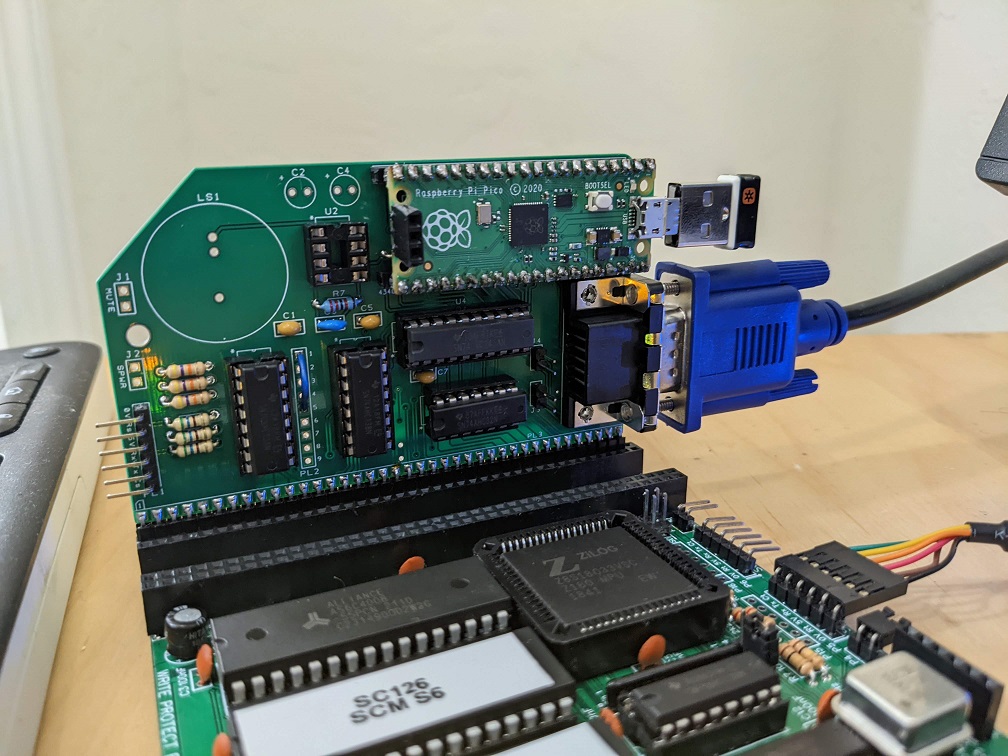
I have a schematic and PCB layout for this project now. The features I plan are RC2014 compatible board, VGA output, audio output, USB HID device input (e.g. keyboard, mouse, gamepad), VT-100 terminal and video display processor with bitmap graphics. Standalone, it could also be used as an ARM single board computer.
Having both a serial port and a Z80 bus interface, it should be useable as VT-100 terminal or Z80 bus connected video display processor or both. The former should allow it to be used with operating system and monitor software having no special driver while the latter offers more features, like bitmap graphics.
My ideas for the VDP are influenced by chips like the VDP-9958 but I don't plan compatibility with any existing chip (though VT-100 has wide support). I want the VDP to have a software interface and graphics capabilities comparable to an 8-bit micro released in 1985. The specifics are a software consideration and can come later.
The audio output is in line with 1980s 8-bit micros: speaker on board, no provision for turning it off and no volume control. The goal is AY-3-8910 compatibility and RomWBW's TUNE.COM working without modification.
Connecting a USB floppy drive is an intriguing possibility but I'm not sure if a Pi Pico can be persuaded to talk to one of those.
The board will not be able to generate wait states, which will motivate me to not use them. My strategy w.r.t. IO requests without wait states is to have the Pi Pico's DMA controller field them rather than one of the ARM cores; the DMA controller has lower latency than an ISR. Let's see if I revise this decision for revision 2!
It will use the original Raspberry Pi Pico as a daughter board with the VGA resistor network underneath to make up for it's large footprint. The Pi Pico will switch to a USB A device and connect to USB HID devices or a USB hub via adapter.
I have no specific questions but feedback before I get boards made would be great.
Schematic and PCB layout attached.
Al
Alastair Patrick
May 24, 2022, 12:48:41 PM5/24/22
to retro-comp
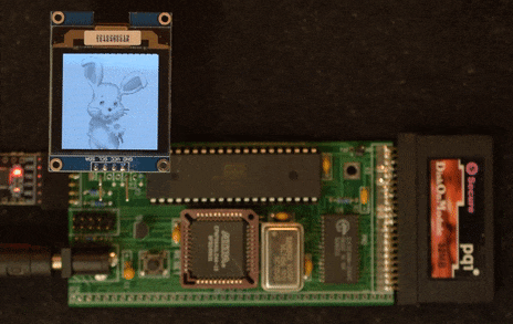
Parts of this project are working. I implemented the VDP card with Z80 bus interface.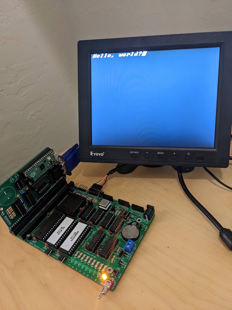
These are the features already working: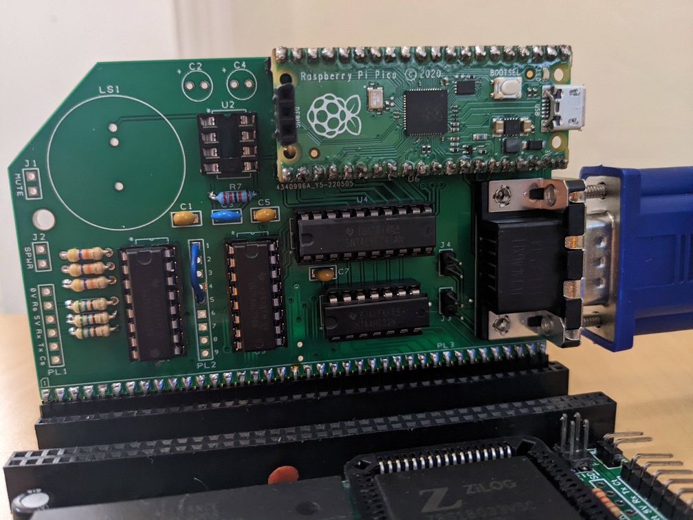
- Bitmap display modes similar to VDP9938: 256x192, 512x192, 2-256 colors
- 16 color, RGB332 palette
- 192KB VRAM
- Z80 bus interface, allowing Z80 computer to set VDP registers and issue blitter commands
- Double buffering
- Hardware 1-pixel horizontal and vertical scrolling
- Hardware blitter
- Blitter save stack, allowing blitter operations to be automatically erased
- One hardware sprite: 16x8, 1 color, hardware blink
- Hardware "copper" effects like on Commodore Amiga, including changing color palette and resolution mid-frame
I haven't started on the VT-100 terminal, audio or keyboard input yet but those seem much easier than the VDP so that's what I'm working on first. I also intend to implement additional blitter commands, sufficient to implement an efficient HBIOS video driver.
The Raspberry Pi Pico was the first thing I had soldered in decades, which is why it's terrible! I'm surprised it still works. I got better at soldering while assembling the SC126 board and my VDP board,
I was able to implement Z80 IO read requests without additional wait states so it's 40-pin RC2014 compatible. It works reliably with a Z180 @18.432MHz and I'm hopeful it will work with a 6MHz or even 10MHz Z80 but that's not tested. The schematic didn't change much from the one I posted earlier; I rearranged some of the address decoding logic to remove a few ns of latency.
Source code, schematic, PCB layout and gerbers are on github.

Kevin Price
May 25, 2022, 11:55:01 AM5/25/22
to retro-comp
That's really neat! I'm especially impressed with your mastery of the PIO. Storing the register being written to/read from in the PIO x&y register is absolutely genius! my pico/z80 thing was way slower because I did a *lot* more with the CPU instead of the DMA . I learned so much from just browsing your code!
Alastair Patrick
May 25, 2022, 10:53:17 PM5/25/22
to retro-comp
Hi Kevin,
What you've done is neat too. Because Dylan replied, I'd already found his posts but I only found yours now. For sure, we're pursuing similar projects.
In a previous life as a game dev, I made graphics engines for Sony Playstation 2 & 3, which involved a deep understanding of those systems DMA controllers. Using the RP2040 PIO that way is a walk in the park compared to getting max potential out of a Sony console back in the day. So unfortunately I'm not a genius. Just an experienced 90-00s game dev.
I think MicroPython is your primary Pi Pico language? I wonder if I could make my design more helpful if it worked with MicroPython? I can program in python. In fact I use it all the time as a language for low traffic web servers. Looking at the PDF schematic from my previous posts, are there any roadblocks preventing a MicroPython programmer using my design?
Al
Al
Kevin Price
May 29, 2022, 1:55:32 AM5/29/22
to Alastair Patrick, retro-comp
Well, if you're not a genius then you're definitely someone who applied themselves to being good at what they did!
I'm honestly not sure if it would work, or what it would take to get it working with micropython - I'd need to really read your code and find out if everything is exposed in the micropython API. I do not see any reason that it wouldn't work so long as the functionality is exposed.
It looks like the main difference is that you use the 74lvc245 to multiplex the data bus and some signal pins. It had only recently occurred to me that you could do that b/c I started playing with the intel 8088.
I did wind up designing a board (no where near as good as yours!). I got a 640x480 text display working with the IBM VGA character rom contents. Then life happened and I haven't been able to make any progress. Most of my approach on the pico side was driven from being able to make heads or tails of the scanvideo library - I spent days working out how FabGL generated vga last summer and then just aped that (dma buffer with hsync/vsync bits on constant loop).
Here's my repo, if nothing else I've got a .h with character rom dumped:
The following link is to a kicad.pcb file stored on the cloud:
I haven't read all of your code, but if you find you need a little extra oomph, the rpi foundation chose a very conservative clock speed.
--
You received this message because you are subscribed to a topic in the Google Groups "retro-comp" group.
To unsubscribe from this topic, visit https://groups.google.com/d/topic/retro-comp/n5j9NgVbNE8/unsubscribe.
To unsubscribe from this group and all its topics, send an email to retro-comp+...@googlegroups.com.
To view this discussion on the web visit https://groups.google.com/d/msgid/retro-comp/a8f36a10-05b1-4614-8158-64977f391b35n%40googlegroups.com.
Alastair Patrick
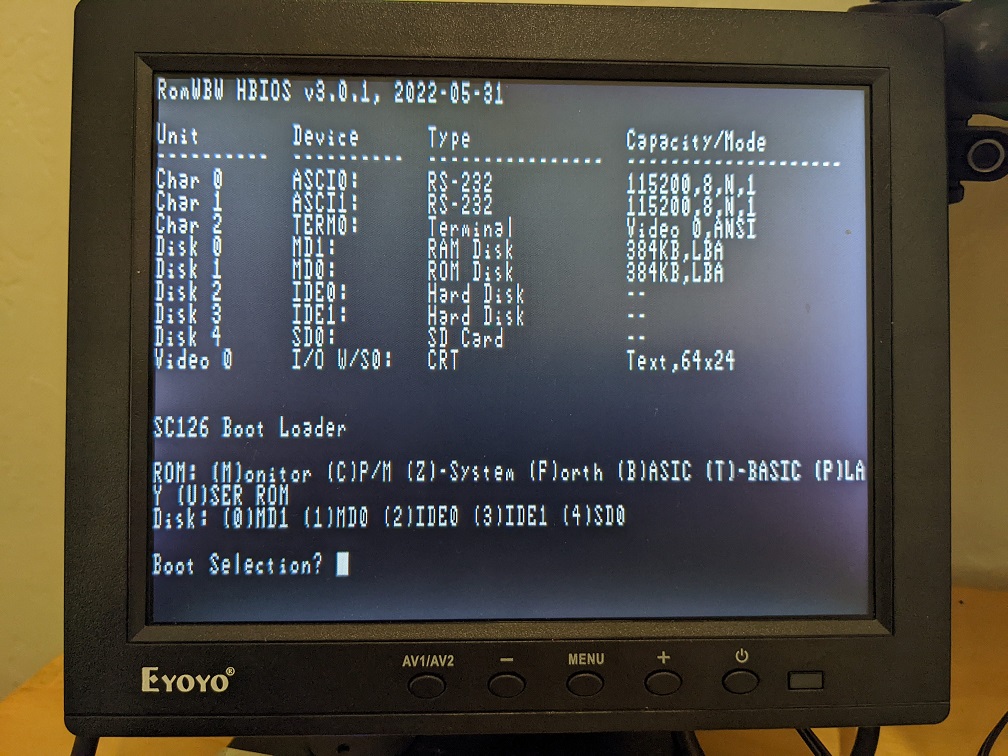
May 31, 2022, 1:43:58 PM5/31/22
to retro-comp
I hooked up a wireless USB keyboard and trackpad. Wireless seems like a good idea: less chance of the board wobbling and I have two input devices without need for a USB hub. USB hubs are supported though.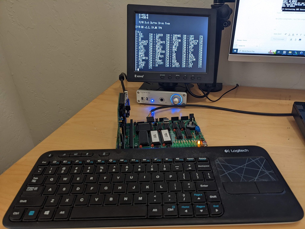
The wireless USB dongle is plugged into Raspberry Pi Pico's USB port. The firmware running on the Pi Pico translates the USB HID events into an MSX-style keyboard matrix visible as registers on the Z80 bus. The HBIOS Visual Display Adapter driver scans the keyboard matrix via those registers. There's no driver for the mouse/trackpad but the X, Y coordinates and button states are visible to Z80 code through registers.
The HBIOS driver provides 64x24 text mode. I've implemented all the VDA entry points and tested all but COPY and FILL. Does anyone know how to exercise the COPY and FILL entry points?
Wayne Warthen
May 31, 2022, 3:05:40 PM5/31/22
to retro-comp
On Tuesday, May 31, 2022 at 10:43:58 AM UTC-7 alastai...@gmail.com wrote:
The HBIOS driver provides 64x24 text mode. I've implemented all the VDA entry points and tested all but COPY and FILL. Does anyone know how to exercise the COPY and FILL entry points?
Excellent progress!
Yes, COPY and FILL are generally the hardest to implement. The COPY entry point is mainly used to implement reverse scrolling. I don't remember where FILL is used, but probably for screen clearing.
Anyway, you can find some minimal documentation on the intended function of all API entry points in the "RomWBW System Architecture" document in the Doc directory of the RomWBW distribution. You want to look at the "VDA" series of functions. Take a look there and then let me know if you still have questions.
I noticed that you are using the current release version of RomWBW (v3.0.1). If you want to submit code updates for RomWBW at some point, please use the "dev" branch of the RomWBW GitHub Repository. All changes are currently going into that branch.
Thanks!
Wayne
Alastair Patrick
May 31, 2022, 8:47:26 PM5/31/22
to retro-comp
I found which ANSI sequences trigger COPY and FILL by reading the ANSI terminal code. WordStar gives them a workout.
I'm happy to submit a patch and I'll put it in the right branch. Let's see if there's any demand first. No reason to complicate the main repository if only one instance of this graphics card exists! I don't plan to make a kit or anything so that's pretty likely what will happen.
Al
Wayne Warthen
Jun 1, 2022, 11:05:19 PM6/1/22
to retro-comp
On Tuesday, May 31, 2022 at 5:47:26 PM UTC-7 alastai...@gmail.com wrote:
I found which ANSI sequences trigger COPY and FILL by reading the ANSI terminal code. WordStar gives them a workout.
Excellent.
I'm happy to submit a patch and I'll put it in the right branch. Let's see if there's any demand first. No reason to complicate the main repository if only one instance of this graphics card exists! I don't plan to make a kit or anything so that's pretty likely what will happen.
Agreed.
Thanks,
Wayne

7alken
Oct 3, 2023, 7:31:09 PM10/3/23
to retro-comp
hi, this PicoVDP is neat! had you measured how much current it draws? I recently ordered very flat 7" hdmi oled 1024x600 display, dreaming about hooking it to some 8bit system, somehow, there is some hdmi out for pico too, but yours "interface chip" looks fine - may be some external simple vga-hdmi bridge possible? but seeking to achieve lowest current drawn... sure;
Petr
Reply all
Reply to author
Forward
0 new messages