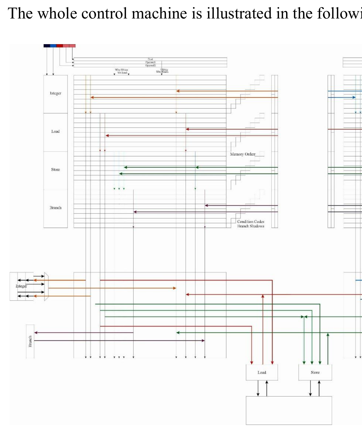
6600-style out-of-order scoreboard designs (ariane)

lk...@lkcl.net
i'm ccing hw-dev as below may prove useful to other people implementing out-of-order designs. i found the PDF overview for ariane which shows that you're implementing (incompletely) a CDC 6600-style out-of-order architecture [1]
if implemented in full you will achieve precise exceptions, need no "rollback" mechanism or "physical-architectural-register-file" nonsense, and yet be extremely power-efficient. this being a known goal of ariane i thought you might appreciate some insights, below.
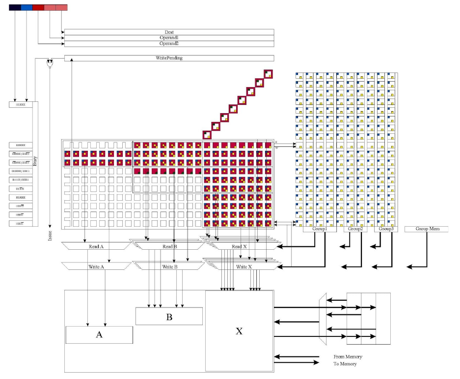
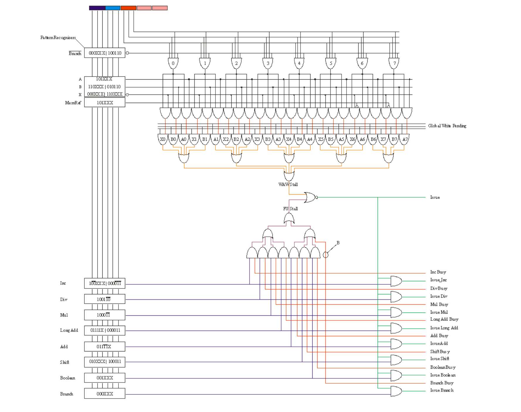
from the CDC 6600 patent (and the academic literature) most people understand that you need a Q-Table, which can be done either as a 1D binary array of register indices, array of length equal to the number of FUs *or* as an unary matrix of bits, N=FUs, M=NumRegs, where in the M dimension only one bit at a time is set [2]
what most people do *not* understand is that you also need an N x N (N=FUs) "dependency" matrix as well, and that in each cell of that N x N matrix there are *multiple* logic blocks handling the commit-blocking signals (write-hazards), those signals usually designated as coming in from the "top", and the usually-expected read hazards coming in from the side, to meet in each cell in an easy-to-lay-out fashion.
no disrespect intended to chris' team (i love the BOOM branch prediction algorithm, chris) listening to chris cello's design advice here will *not help you* because his team have implemented the TOMASULO algorithm, which involves a Reorder Buffer, which in turn means they need a CAM, and that is severely power-hungry.
although the Tomasulo algorithm is topologically equivalent to a (properly implemented) 6600-style algorithm, the topological morphing required [3] leaves very little that either design may use - or learn - from the other (without a full comprehensive study of both)
the 6600-style algorithm is extremely power-efficient, requires far less gates, and *does not need CAMs*. instead it uses unary or binary array encoding as a DIRECT substitute for a CAM, providing exactly the same end-result, and only needing a single AND gate to indicate "active detection".
a CAM cleary requires *multiple* AND gates... *PER ENTRY* in the array.
thus it is clearly far more power-efficient to use 1D-binary-array or 2D-unary encoding.
each cell in the N x N Dependency Matrix basically combines in an OR fashion its write hazard lines (commit-blockers). those commit-blockers may be:
* exception blockers. these also handle interrupts.
* branch speculation commit-blockers
* LD/ST blockers (LD/ST management is best done as its own OxO matrix that then feeds its write-hazards to the NxN one)
* "the usual" register-based result blockers (write hazards) which everyone thinks, from the academic literature (and the expired patents) on the 6600, is the only thing that scoreboards can be used for [hint: it's not].
* exception blockers basically stop all down-stream instructions from committing. once the instruction that *MIGHT* have to throw an exception *KNOWS* that it does not need to throw an exception, it drops its write-hazard line. if it does, it throws the "Go-Die" switch on down-stream instructions. in this way you get PRECISE exceptions. ta-daaaa.
* interrupts *as* an exception means that you *do not* need to do global masking. commit-blocking on exceptions (interrupts) *is* in effect "masking" [selectively]. it's directly functionally equivalent, yet the "masking" idea that you described last week, Florian, is the "Nuclear Option", blasting away all and any possibility of *any* interrupts.
* branch speculation commit-blockers basically also hook into the "go-die" (instruction cancellation) capability that is needed for clearing out the Function Units if an exception occurs. i nick-named it the "Schroedinger wire" :) at the branch-speculation point, you very simply hold a commit-block on all down-stream instructions (in *both* paths if you choose to do that), and when the branch is known to be taken, you either drop the write-hazard or you call the "go-die" (instruction cancel) wire.
* LD/ST blockers, they require their own separate OxO (very-sparse) matrix, with their own sparse-array of hazards (down the main diagonal): LDs block stores, and STs block LDs. *both* the LD and ST write-commit-blocker signals drop down from above, into the *NxN* Dependency Matrix.
* you have the "usual" register-based write-blocking, and also (which i really like), you have operand (result) forwarding automatically built-in. however, you have added logic that detects whether an exception has occurred into the operand forwarding block... where, actually, as you can see above, exceptions *need* their own write-hazards, and once cleared, it will be SAFE to forward the operands.
in scoreboard.sv i am not seeing any evidence of the combining of those signals, meaning that you are running into the very difficulties with exceptions (interrupts) that you outlined last week on the list, and you will also be running into difficulties with LD and ST.
i did note that you have a per-FU instruction-in-flight counter, which is excellent. the reason why is because these counters can be used to turn this into a multi-issue design very very easily. you very simply:
* count up the number of FUs ready to "commit" (that have no hazards remaining) - using a popcount
* set a threshold of the number that are *ALLOWED* to commit
* if the per-FU instruction-in-flight counter is less than this threshold, allow commit!
* count up the number that were *actually* committed...
* subtract that global count from EVERY one of the per-FU instruction-in-flight counters.
then all you need do is extend the instruction decode and issue phase to drop more than one result into the system: ta-daaa, now you have turned a single-issue design into a multi-issue one :)
of course the multi-porting on the operand forwarding will go up, and the multi-porting on the register file will go up as well: in the Libre RISC-V SoC we stratify the register file (and double/quadruple the number of FUs as well, to match) to avoid this.
this approach has the rather weird side-effect that one from each of register result modulo 4 may be multi-issue committed in any given cycle. by that i mean that if there are operations which can commit to r4, r8, r12 and r16, these MUST be done sequentially (in 4 cycles), however if we have operations which can commit to r1, r6, r3 and r8 (modulo 4 those are 0,1,2,3), that's okay because of the 4-bank stratification.
it's a little weird however it means that we can use 4x 32-deep banks of 3R1W SRAM instead of requiring a *COMPLETELY INSANE* 256-entry 64-bit 12R4W ported SRAM.
anyway, above is some insights that will help you to avoid a *lot* of design pain, and, if implemented, will give you a stonkingly-good power-performance ratio, for very little effort, and without having the kinds of compromises *normally* expected of a Tomasulo (ROB) algorithm *or* of what is *believed* (incorrectly) that a 6600-style architecture is only capable of.
lk...@lkcl.net

Florian Zaruba
hiya florian, appreciate that you're busy with current tasks - i spotted a potential major design flaw that... how can i put this... "could be the cause of the very debugging and investigation tasks that i surmise may be preventing you from having the time to evaluate mitch alsup's book chapters and the information that i am providing on 6600-style scoreboard design" shall we say.
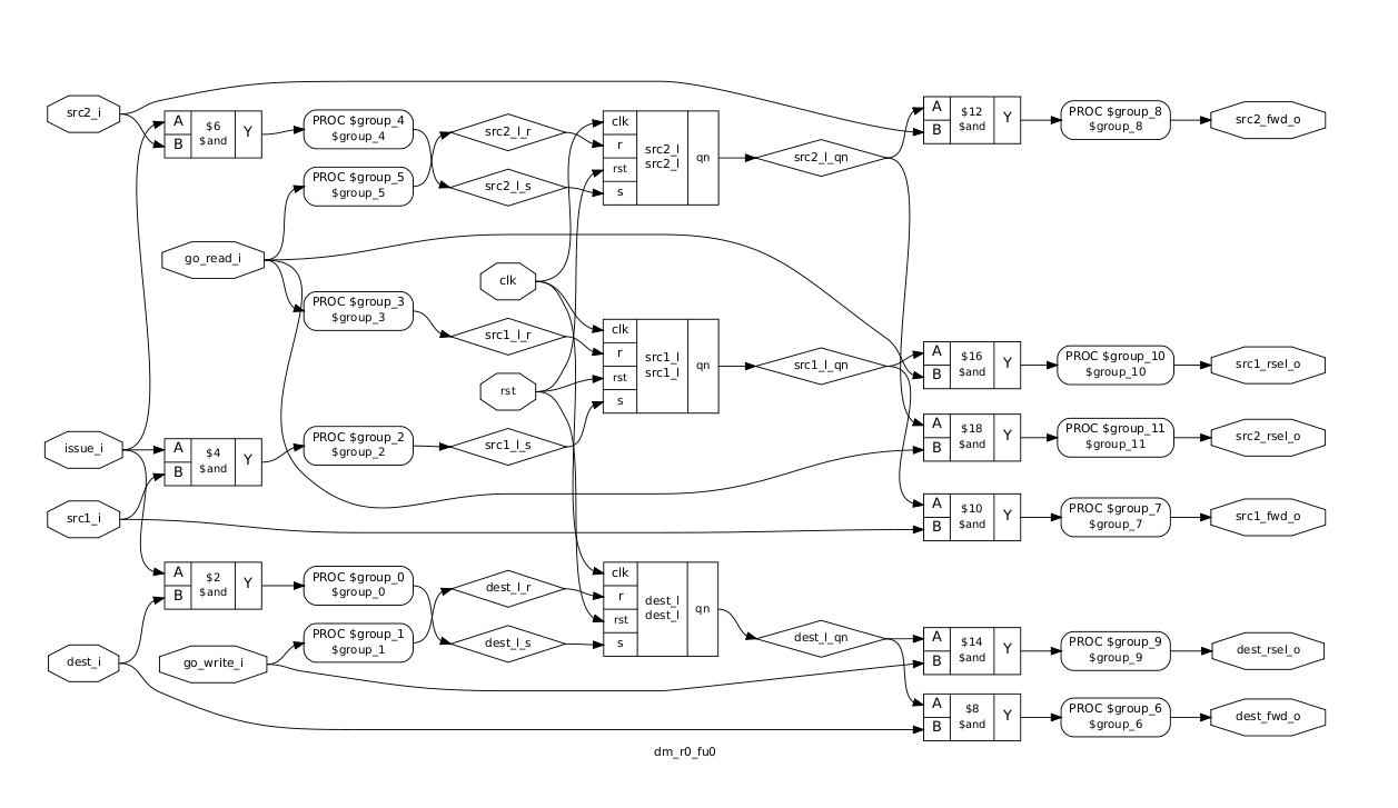
register-renaming (and built-in operand forwarding) is automatically achieved with the 6600-style scoreboard design by way of the Q-Table working along-side the NxN Function Unit Dependency Matrix. operand forwarding in the 6600 was achieved by using same-cycle (actually, falling-edge) write-through capability on the Register File. in modern processors, "write-through" of SRAMs can be used for this exact same purpose. this *can* be augmented by a separate additional operand-forwarding bus, very similar to an SRAM except... without the SRAM.also, pipelining in the 6600 was sort-of achieved by a "revolving door" created by the three-way interaction between Go_Read (register file read), Go_Write (Function Unit latch write) and Go_Commit [write to regfile, i think: mitch can you confirm?]. only two of these signals were permitted to be raised at any one time, and only when one of them was HI could the next-in-the-chain go HI, at which point the previous one would drop, hilariously a bit like a very short caterpillar going round in circles, forever. operand-forwarding was achieved when two of these lines (one of them Go_Read) were HI for example.the important thing is that actual pipelining was not introduced until the 7600, not many details are known about the 7600, however the Function Units input-latches and corresponding associated output-latch had this "revolving door" 3-way MUTEX on each of them *even in the 7600*.in the creation of the ariane scoreboard.sv, however, there is a problem, that is masked / hidden by the fact that the integer ALU operations are all single-cycle.* on the div unit, you *do* have a form of MUTEX that blocks the Function Unit input operands from being used whilst the DIV operation is in progress. you will therefore not experience any problems with DIV results.* on the integer FUs, these are single-cycle, so the problem is *HIDDEN*. note however there will also be a performance ceiling (64-bit MUL in a single cycle) due to gate latency, that, if fixed by creating a multi-stage integer-mul, *WILL* result in problems.
* on the LD/ST FU, you *may* see problems. i haven't investigated in depth, because the design is deviating from the 6600 by not splitting out LD/ST into its own separate sparse-array matrix (see section 10.7)* on the FPU FUs, which i see no evidence of a MUTEX, and i assume that they're multi-stage, you *WILL* experience problems.
the problem is: that without MUTEXes blocking the Function Unit from re-use until the output is generated, the Q-Table will become corrupted. this will show up *ONLY* during exceptions (and possibly branch speculation cancelling), because it is exceptions where rollback is initiated.
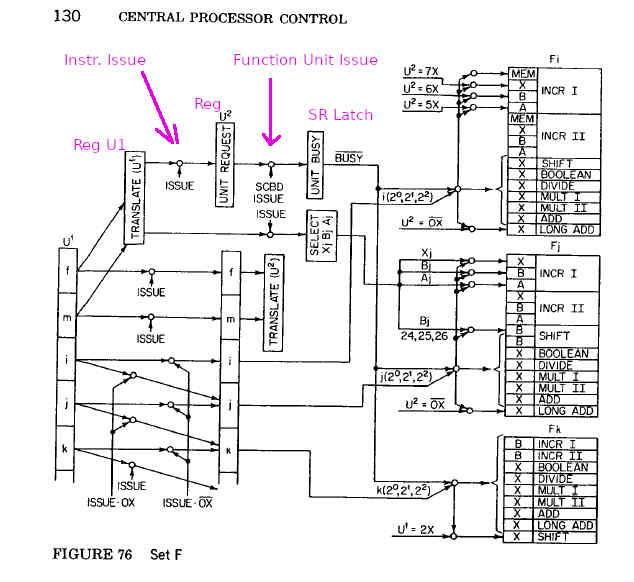
when a destination (result) register number is transferred through the Q-Table to a Function Unit, it does so by assuming that there is a commit-block on that register which "preserves" the name of that destination register. this is sort-of done by preventing its destruction using the write-hazard infrastructure until such time as its committing can "make it disappear" safely.thus: only when that result is *actually available* is it SAFE to DESTROY (retire) that result, because at the point at which the result is stored, all "commits" - all write hazards - have been cleared.by allowing the Q-Table to proceed to a new entry without allowing the write-hazards to be cleared, you are DESTROYING absolutely CRITICAL information.i repeat:by allowing the Q-Table to tell the Function Unit that the write-hazards do not matter, rollback is NO LONGER SAFELY POSSIBLE.the solution is outlined in Section 11.4.9.2 of mitch's book chapters. reproduced with kind permission from mitch alsup, an image for people who may not have these chapters:you can see there that there are *four* "apparent" Function Units, all with src1, src2 operand latches, and associated corresponding result latches, so it APPEARS as far as the NxN Function Unit Dependency Matrix that there are FOUR adders (or four FPUs).there are NOT four FPUs.there is only ONE (pipelined) FPU.that FPU however has *FOUR* sets of src1-src2-result latches.the absolutely critical insight here is to note that the number of FU latch-sets *must* exceed or be equal to the pipeline depth.* if it is less, the consequence will be that the pipeline will be underutilised.* if it is greater, there exists the increased ability of the design to undergo register renaming, however bear in mind that the FU NxN Dependency Matrix is, clearly, O(N^2).one solution in common usage is to merge multiple functions into the Computation Unit, funnily enough exactly as has already been done in both the ariane FPU Function Unit and the ariane integer ALU.you will be able to check that this is the case by temporarily creating a global "de-pipelining" mutex that only permits a single operation to be carried out at any one time. only one of an FPU operation, LD/ST operation, Branch operation or Integer operation may be permitted at any one time, *NO PIPELINING PERMITTED AT ALL*...... and at that point the problems that i anticipate you to be experiencing (based on an examination of this design) on exceptions and branch prediction should "puzzlingly and mysteriously disappear for no apparent reason".
we have an implementation of a multi-in, multi-out "fan" system in nmigen (if you're able and happy to read python HDL), at least the comments are useful:the "mid" - multiplexer id - is what is passed in down the pipeline, just as ordinary boring unmodified data, only to be used on *exit* from the pipe to identify which associated fan-out latch the result is to go to.that mux-id is used here for example:you can see later at lines 202, 203, 204 and 208, the mid indexes which of the "next stages" to route the incoming data to. i really like nmigen :)in the diagram in Mitch Alsup's book you can see that this is replaced with a FIFO (just to the side of the Concurrent Unit aka pipeline). however that particular design strategy works for a fixed-length pipeline, i.e. it *prevents* early-out and it *prevents* the amalgamation of multiple pipelines (with different lengths) behind a common "ALU" API.
by passing the multiplexer id down through the data, early-out, reordering pipeline layouts, *and* FSMs can all be combined and the multi-in multi-out Concurrent Unit doesn't give a damn :)early-out pipelines (such as FPU "special cases" for NaN, zero and INF being handled very early in the pipeline) allow less work to be done (less power utilised), however it would be anticipated that this would require dual-porting on the result stage (into the multiplexer). luckily however we *guarantee* that only *one* of the array of result stages is ever going to be active at any one time, so, bizarrely, ORing of the two possible paths may be deployed as opposed to requiring higher gate count MUXes.
two fan-outs will still be required (one for the early-out path on the FPU pipeline, one for the "normal" path on the FPU pipeline), it's just that the fanned-out outputs from each may be safely ORed together, given the *guarantee* that there will be only one mid in use at any one time.so... i think that covers it. summary: you're missing criticical MUTEXes on the Function Unit src1-src2-result latches, without which data corruption will occur (guaranteed) on any form of rollback. fix that, and you'll have an absolutely fantastic design.
Florian
l.
lk...@lkcl.net
On Friday, April 19, 2019 at 2:49:22 PM UTC+1, Florian Zaruba wrote:
Dear Luke,thanks for all the suggestions and the book chapter.On Fri, Apr 19, 2019 at 3:22 PM <lk...@lkcl.net> wrote:hiya florian, appreciate that you're busy with current tasks - i spotted a potential major design flaw that... how can i put this... "could be the cause of the very debugging and investigation tasks that i surmise may be preventing you from having the time to evaluate mitch alsup's book chapters and the information that i am providing on 6600-style scoreboard design" shall we say.Unfortunately, this is not the reason as I still have to pursue a PhD degree (and you won't get that solely with engineering an in-order core) ;-).
I appreciate your input and I have the two book chapters as my easter lecture. I hope they will be insightful.
... and at that point the problems that i anticipate you to be experiencing (based on an examination of this design) on exceptions and branch prediction should "puzzlingly and mysteriously disappear for no apparent reason".I am actually not experiencing any more problem: The "design flaw" which produced the buggy behavior of non-idempotent reads was associating interrupts during commit. The observation to do that during decode helped to eliminate that problem. We are happily booting Debian Linux on the FPGA and multi-core SMP Linux on the OpenPiton platform (with PLIC).
early-out pipelines (such as FPU "special cases" for NaN, zero and INF being handled very early in the pipeline) allow less work to be done (less power utilised), however it would be anticipated that this would require dual-porting on the result stage (into the multiplexer). luckily however we *guarantee* that only *one* of the array of result stages is ever going to be active at any one time, so, bizarrely, ORing of the two possible paths may be deployed as opposed to requiring higher gate count MUXes.Our FPU manages all that.
so... i think that covers it. summary: you're missing criticical MUTEXes on the Function Unit src1-src2-result latches, without which data corruption will occur (guaranteed) on any form of rollback. fix that, and you'll have an absolutely fantastic design.One "problem" which I have, is this merged scoreboard/rob structure (as it is quite area and timing critical).
I have the possibility to rollback the entire state speculative state so no data corruption can occur ;-)
But I am certain that the current design point can be further improved. I am hoping that the lecture you send me is giving further insights.

k...@dspia.com
lk...@lkcl.net
Hi Luke,so I've taken the time and read the pages you have sent me, thanks again. It contains some neat tricks.
I am still a bit confused on a couple of things:1. The paper mentions a 8r/4w register file.. That seems quite unnecessary big for a single issue core.
You won't retire much more than one instruction and definitely not read more than two operands (let us concentrate on the integer part). Even for a dual issue approach, you read approximately 1.5 registers per instruction. So three ports should be sufficient.
Not a big deal I think that can be circumvented by some read/write port handshaking on the regfile
.2. Unfortunately, the drawings are quite hard to read as they are blurry pixel graphics
and the style is not very consistent or self explanatory I am sure I missed a couple of points there.
Also, there seem to be transmission gates in the drawings which I think are meant to be some kind of storage (flip-flops)..
3. The text talks about continuous scoreboard and dependency matrix scoreboard.
The former seems to be a distributed version which takes all the information from the reservation stations/FU and generates global signaling. Does it require extra storage somewhere centralized or can everything be computed combinatorial?
Although not entirely clear from the text it seems that the continuous scoreboard is preferable.
4.. What information exactly does the reservation station/FU need to contain?
I assume from the drawings that it also needs to capture the write data from the computation unit.
5. I am desperately missing a high-level diagram on how the different things fall in place.
6.. The text talks a lot about latches. I am not sure whether latches in the circuit sense are meant.
If so I would recommend you to take a different approach. Some text also indicates that you are making use of the transparent phases of latches. This all seems rather dangerous.
7. One part of the text (11.1.1) talks about instructions can enter the FUs even if they have WAW hazards, it juts needs to make sure it doesn't write its result back until the WAW hazards has been cleared.
The rest of the text talks about issue stalling if a WAW hazard has been detected.
8. What does "issue" actually mean?
Does it mean putting it in the reservation/station FU?
Or does it mean bringing it to the next stage aka read operands?
The image in 11.3.1 seems to indicate the former. Do you really have to keep a separate queue of unissued instructions?
What prevents you from putting them in the reservation station and marking them as "not issued"?
9. I am not really getting the placement of read reservations. If an instruction is being issued it places read and write reservations.
If the instruction unconditionally places a read reservation you are throwing away the temporal relationship?
How do you maintain order on the read operands if you issue out of order (e.g. if you defer issuance of one instruction which would be vital for the correct dependency)? In general how do you keep a "temporal order"?
Maybe if I'd know the exact fields of the scoreboard that would help me understand it.

高野茂幸
--
You received this message because you are subscribed to the Google Groups "RISC-V HW Dev" group.
To unsubscribe from this group and stop receiving emails from it, send an email to hw-dev+un...@groups.riscv.org.
To post to this group, send email to hw-...@groups.riscv.org.
Visit this group at https://groups.google.com/a/groups.riscv.org/group/hw-dev/.
To view this discussion on the web visit https://groups.google.com/a/groups.riscv.org/d/msgid/hw-dev/ce05d1d6-67f3-45fb-a852-8174424dbb83%40groups.riscv.org.
Dr Jonathan Kimmitt
See comments inline Luke and best of luck with your
implementation. I would recommend that you turn those schematics
into a Verilog simulation model (it supports T-latches which are
called tranif0/1 devices. Depending on the usage it may result in
so-called registered nets that have an impact on simulation
speed).
Quite possibly.... although in talking with Mitch he explained that only D latches are needed (3 gates). Flip flops (10 gates) are usually used by non-gate-level designers because they're "safe" (resettable).
And have a high cost.
3. The text talks about continuous scoreboard and dependency matrix scoreboard.
Yes. They are definitely separate.The former seems to be a distributed version which takes all the information from the reservation stations/FU and generates global signaling. Does it require extra storage somewhere centralized or can everything be computed combinatorial?
It looks that way! It really is much simpler than we have been led to believe.You can confirm this by examining the original circuit diagrams from Thornton's book.
Yes, the full gate level design is in that book. It's drawn using ECL as they literally hand built the entire machine using PCBs stuffed with 3 leg transistors you can buy from RSOnline, today!
Although not entirely clear from the text it seems that the continuous scoreboard is preferable.
Yes.
4.. What information exactly does the reservation station/FU need to contain?
Nothing! It's a D Latch bank! That's it! Latches for the src ops, latch for the result, and ... errr... that's it.Mitch and I had a debate about this (details), happy to relate when you have time.
I assume from the drawings that it also needs to capture the write data from the computation unit.
Yes.5. I am desperately missing a high-level diagram on how the different things fall in place.
Believe it or not, it is so much simpler than you may have been led to believe, the diagram on page 32 chap 10 *really is everything that is needed*
Or p28 or p30. Different highlighting on different sections.
6.. The text talks a lot about latches. I am not sure whether latches in the circuit sense are meant.
Yes D latches. Really D latches. Not flip flops.
If so I would recommend you to take a different approach. Some text also indicates that you are making use of the transparent phases of latches. This all seems rather dangerous.

Samuel Falvo II
(with thanks to Florian for kindly agreeing to publish what was formerly a private discussion, this may be of benefit to others in the future. i'm also attaching two key screenshots, reproduced with kind permission from Mitch Alsup. discussion edited slightly).
Samuel Falvo II
... sounds all very obvious so far, right? :) now the tricky bit:
lk...@lkcl.net
lk...@lkcl.net
| Apr 26, 2019, 10:33 PM (2 days ago) | |||
lk...@lkcl.net
Dr Jonathan Kimmitt
A write-through RAM is an optimised bit-cell (equivalent to a
D-latch) surrounded by sense amplifiers. Logically it is
equivalent to a latch, but it would be in no way competitive with
a latch in area or power consumption. Also in UDSM technologies
RAMs may require a threshold margin optimisation control as well
as optional BIST circuitry, which I guess is the part that is
interesting for you.
--
You received this message because you are subscribed to the Google Groups "RISC-V HW Dev" group.
To unsubscribe from this group and stop receiving emails from it, send an email to hw-dev+un...@groups.riscv.org.
To post to this group, send email to hw-...@groups.riscv.org.
Visit this group at https://groups.google.com/a/groups.riscv.org/group/hw-dev/.
To view this discussion on the web visit https://groups.google.com/a/groups.riscv.org/d/msgid/hw-dev/00fde2ca-2085-4e65-ac78-9c123d74f34a%40groups.riscv.org.

Dan Petrisko
--
lk...@lkcl.net
On Wednesday, May 1, 2019 at 3:29:10 PM UTC+1, Dan Petrisko wrote:
For very small, simple structures, logic elements are vastly more efficient than SRAMs.
Dr Jonathan Kimmitt
SRAMs will have a word line which goes to all relevant content
(i.e. the corresponding bits in the word), but if N is less than
some magic, but quite large threshold then using an optimised bit
cell is so not worth it. Now the more interesting question is what
size of register file would be needed to justify a dedicated
register file IP. This will of course depend on the number of
simultaneous ports in use. A large number of ports will degrade
timing because of the number of word lines hanging off each cell.
For more details refer to (for example) Chapter 9 of "Fundamentals
of Modern VLSI Devices" by Yuan Taur and Tak H Ning. My
understanding is that you are planning to have a register file
with a large number of ports.
--
You received this message because you are subscribed to the Google Groups "RISC-V HW Dev" group.
To unsubscribe from this group and stop receiving emails from it, send an email to hw-dev+un...@groups.riscv.org.
To post to this group, send email to hw-...@groups.riscv.org.
Visit this group at https://groups.google.com/a/groups.riscv.org/group/hw-dev/.
To view this discussion on the web visit https://groups.google.com/a/groups.riscv.org/d/msgid/hw-dev/5e482cbe-1a0e-43e5-bbf8-7a12767d0cee%40groups.riscv.org.
lk...@lkcl.net
On Thursday, May 2, 2019 at 9:18:36 AM UTC+1, Dr Jonathan Kimmitt wrote:
SRAMs will have a word line which goes to all relevant content (i.e. the corresponding bits in the word), but if N is less than some magic, but quite large threshold then using an optimised bit cell is so not worth it. Now the more interesting question is what size of register file would be needed to justify a dedicated register file IP. This will of course depend on the number of simultaneous ports in use. A large number of ports will degrade timing because of the number of word lines hanging off each cell. For more details refer to (for example) Chapter 9 of "Fundamentals of Modern VLSI Devices" by Yuan Taur and Tak H Ning. My understanding is that you are planning to have a register file with a large number of ports.
lk...@lkcl.net
lk...@lkcl.net
http://ygdes.com/CDC/DesignOfAComputer_CDC6600.pdf
https://archive.org/details/cdc.6600.thornton.design_of_a_computer_the_control_data_6600.1970.102630394_201802
------------------
In the CDC 6600::The Global issue signal causes the instruction fetch/decode pipeline to advance.
The Global issue signal ANDED with the <empty> FU decode (image) causes the
issued instruction to be latched in the Function Unit and in the Computation Unit.
Also note: in the CDC 6600, due to the use of latches, if the instruction is not issued,
the fetch/decode pipeline advances but recognized the instruction was not issued.
The advanced instruction remains undecoded, and a mux redecodes the advanced
instruction until issue is successful.
See Thornton page 122.
lk...@lkcl.net
> Note: I was describing how CDC 6600 did it.
> There may (hint: MAY) be better ways with today's technology (clocked flip-flops,
lk...@lkcl.net
> > nmigen! python! modern OO programming! classes n random stuff that's actually human-readable!
高野茂幸
--
You received this message because you are subscribed to the Google Groups "RISC-V HW Dev" group.
To unsubscribe from this group and stop receiving emails from it, send an email to hw-dev+un...@groups.riscv.org.
To post to this group, send email to hw-...@groups.riscv.org.
Visit this group at https://groups.google.com/a/groups.riscv.org/group/hw-dev/.
To view this discussion on the web visit https://groups.google.com/a/groups.riscv.org/d/msgid/hw-dev/fe8afe03-b2f3-410c-85e2-6204edf12179%40groups.riscv.org.
lk...@lkcl.net
On Sunday, May 5, 2019 at 1:53:15 AM UTC+1, adaptiveprocessor wrote:
Hi Luke-san,Off topic:
Rather than company does with closed code set, open software tool remains opportunity to succeed after leave of owner, it is healthy.
I use chisel3.0 for my project, it generates so many intermediate wires, therefore, trace-check the generated code takes unnecessary time.
I will try using the nmigen, thank you for your info.
Still now, use of product tools is common sense. It is ok when company work, they have a responsibility for users under license. Ordinary users do not care of earth quake, and spend every day. Means difficulty of explain the moving shift to open source, especially companies of potential user.
高野茂幸
--
You received this message because you are subscribed to the Google Groups "RISC-V HW Dev" group.
To unsubscribe from this group and stop receiving emails from it, send an email to hw-dev+un...@groups.riscv.org.
To post to this group, send email to hw-...@groups.riscv.org.
Visit this group at https://groups.google.com/a/groups.riscv.org/group/hw-dev/.
To view this discussion on the web visit https://groups.google.com/a/groups.riscv.org/d/msgid/hw-dev/4d828363-53c0-4f5b-8a61-756448ead7e1%40groups.riscv.org.
Samuel Falvo II
> however... i honestly found that outputting to yosys "ilang" format, then using yosys "read_ilang {filename.il}; show top" was far more productive and useful than reading the actual (auto-generated) verilog.
to be a bug, but I'm sure is just a misunderstanding on my part.
If I have nmigen code like this:
ctr = Signal(COUNTER_WIDTH, reset=DEFAULT_VALUE)
m.d.sync += output_port.eq(ctr)
without further qualification or use of `ctr`, then it seems that
nmigen will yield a proper, constant-valued register which simulates
properly in Verilator, but which will be treated as an *anonymous
module input* when used with formal verification. This latter
distinction is important, because the formal prover software will
freely fuzz inputs during k-induction proofs unless somehow
constrained with Assume statements. But, in this particular context,
assumptions would be the wrong thing; I'm *specifying explicitly* what
I want in the HDL itself. So, how to fix this?
The work-around for this, I've found, is easy to apply: you just force
the register to equal itself, like so:
ctr = Signal(COUNTER_WIDTH, reset=DEFAULT_VALUE)
m.d.sync += [
output_port.eq(ctr),
ctr.eq(ctr),
]
This is enough to trick the ilang backend into realizing that ctr is,
in fact, driving *something*, and so is a real register, and not an
input port.
However, I *never* would have found this were it not for looking at
the generated schematic. Because, in the schematic, if ctr appears in
an octagon, you *know* it's treated as an I/O port.
DISCLAIMER: You probably won't run into this edge case because most
designs don't instantiate fixed-value registers like this. I,
obviously, intend on replacing this with more complex logic later on.
But, since I'm very early in my development cycle, I don't yet have
everything I need to do so, I "stub" out a portion of my circuit with
a hard-wired register, like this.
Still, it meant the difference between formal properties never being
met versus formal properties which properly match my happy-path unit
test behavior.
> * unit tests are ABSOLUTELY ESSENTIAL. if you cannot accept this (think you know better, "i'm a good programmer, i don't need to write unit tests"), you will take ten times as long as anyone else... that's if you succeed at all.
Not only are unit tests essential, the whole test-driven development
process would, in my opinion, be essential. It's far too easy to
write code which doesn't have adequate coverage otherwise. *More* of
my time yesterday was invested into researching why my formal
properties *didn't* fail in the expected way than I spent in making
them pass. I found at least as many bugs, if not more, this way than
just making the bare minimum amount of tests pass.
Also, if your tools support it, I'd advocate using formal methods in
conjunction with unit tests. Contrary to what many think, I find they
*compliment* each other. Formal is great for proving fundamental
properties of a circuit, while unit testing is great at proving more
sophisticated or stateful interactions. The same unit test framework
is also used for integration testing as well. I approach this by
follow this crude procedure:
1. Write a unit test for some feature I desire. Make sure this unit
test FAILS. If it doesn't fail, you either duplicated work somewhere,
or some other assumption about your code is wrong. Re-evaluate your
code and requirements to make sure they agree with each other.
2. Write just enough nmigen code to make the test pass.
At this point, I have a circuit that fulfills my requirements so far.
However, this doesn't mean that the circuit is *correct*. It just
means that it (perhaps by accident) fulfills my documented
requirements.
3. Write formal properties which covers the new behavior you just
tested. These will be a subset of the formal properties of the
circuit. And, in some sense, you're duplicating work. But it's
essential this be done, because it also helps constrain the formal
prover's search space.
4. Write additional formal properties that covers various edge cases.
For example, in my TileLink code, I always separate address from data
phases in time, so a_valid and d_ready are never asserted at the same
time. I also have properties to ensure proper sequencing as well, so
that d_ready always asserts *after* a_valid negates, or that both
a_valid and d_ready are both negated after reset. Etc. Here's the
biggest pay-off from using formal verification in conjunction with
unit tests. It not only saves you from having to write a ton of
negative unit tests, it does a far better job of finding the edge
cases for you than you ever could (think of k-induction proofs as
guided input fuzz testing). This leaves your unit tests to (more or
less) happy-path only code, which is always much easier to read and
use as examples (in the sense of, "How do I do ...?") for
documentation later on.
5. Commit your code with full confidence that it meets your
understanding of the requirements at that time, then repeat as
necessary. Each iteration of this loop will result in a design being
refined over time until it finally meets the product requirements as a
whole. NOTE: You might even find cases where the requirements are
inconsistent, and will need to alter them before proceeding. But,
then, that's software engineering in a nutshell, and probably all of
engineering in general anyway.
lk...@lkcl.net
On Sunday, May 5, 2019 at 4:44:27 PM UTC+1, Samuel Falvo II wrote:
On Sat, May 4, 2019 at 7:24 PM <lk...@lkcl.net> wrote:
> however... i honestly found that outputting to yosys "ilang" format, then using yosys "read_ilang {filename.il}; show top" was far more productive and useful than reading the actual (auto-generated) verilog.
I actually had to do this just last night to discover what I consider
to be a bug, but I'm sure is just a misunderstanding on my part.
If I have nmigen code like this:
ctr = Signal(COUNTER_WIDTH, reset=DEFAULT_VALUE)
m.d.sync += output_port.eq(ctr)
However, I *never* would have found this were it not for looking at
the generated schematic. Because, in the schematic, if ctr appears in
an octagon, you *know* it's treated as an I/O port.
a_valid and d_ready are both negated after reset. Etc. Here's the
biggest pay-off from using formal verification in conjunction with
unit tests. It not only saves you from having to write a ton of
negative unit tests, it does a far better job of finding the edge
cases for you than you ever could (think of k-induction proofs as
guided input fuzz testing). This leaves your unit tests to (more or
less) happy-path only code, which is always much easier to read and
use as examples (in the sense of, "How do I do ...?") for
documentation later on.
lk...@lkcl.net
lk...@lkcl.net
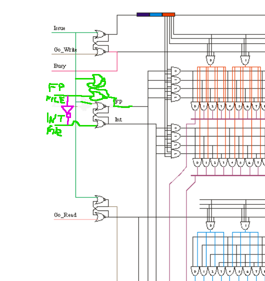
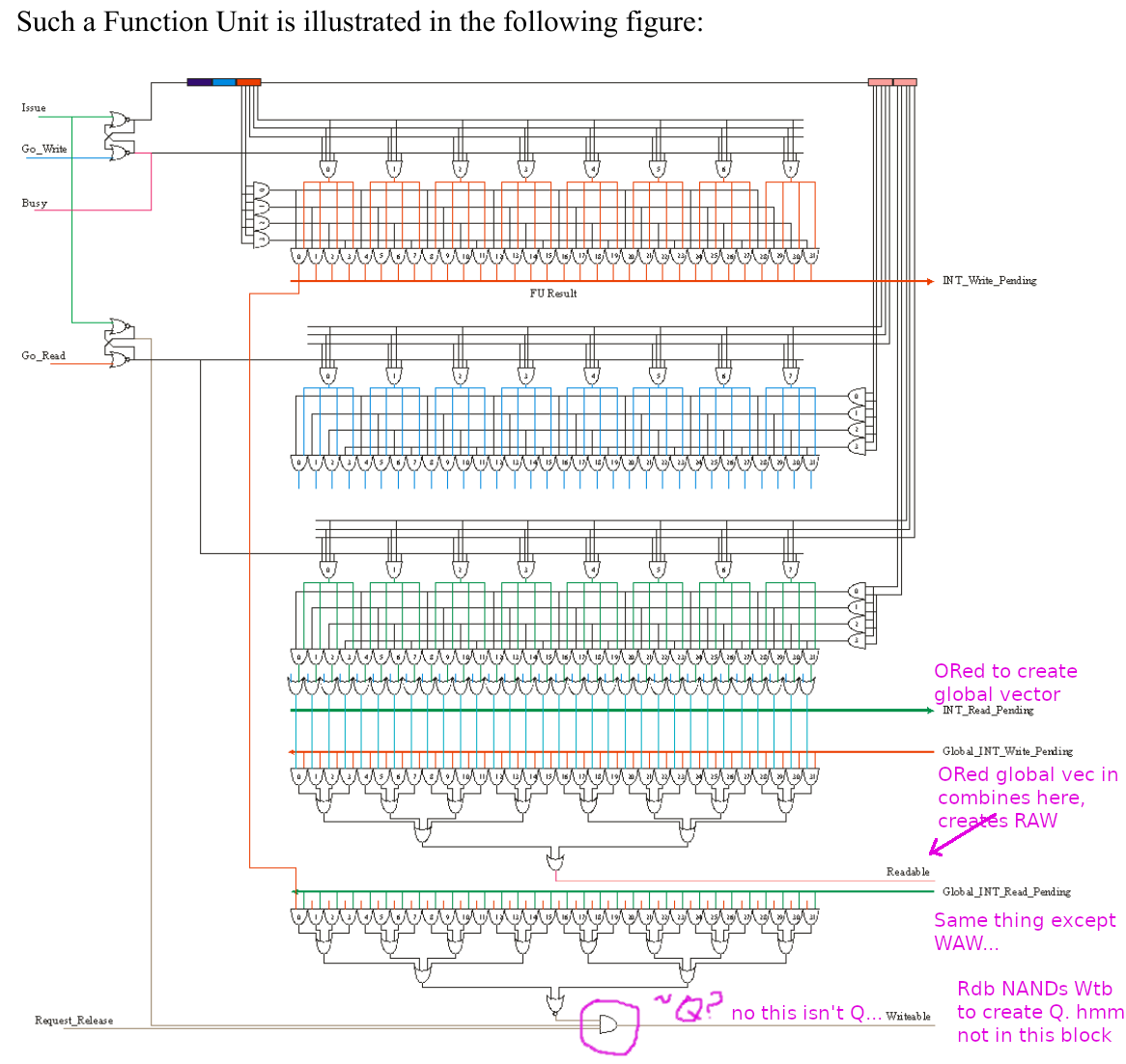
> Let me clarify:: What you see in the drawing is one function unit and in this case we can see on the
> right hand side that this is the INT function unit. So the Issue, GO_Read and Go_Write should really
> be Issue_INT, Go_Read_INT, and Go_Write_INT. The FPU will have a similar one covering all the
> FP registers. {ANd of course: Busy_INT.} You don't comingle register data-flow INT<->FP.
>
> Secondly: ISSUE_INT, Go_Read_INT, and Go_Write_INT are unarily assertions.
>
> So: Go_Write_INT clears the "I have an Instruction" SR-flop enabling a ISSUE_INT in some future
> cycle.
>
> Issue_INT: sets the "I have an Instruction" SR-flop which drives the Busy_INT signal.
>
> Go_Read_INT: sets the "Operands have arrived" SR-Flop and signals Writeable
>
> Go_Write_INT clears the "I have an Instruction" SR-flop enabling a ISSUE_INT in some future
> cycle. And the cycle repeats.
>
> Note: This is "the" degenerate Function unit that knows each of its instructions are 1 cycle.
>
> The Go_Read_X and Go_Write_X are asserted by Pickers (FF1s) on clock boundaries.
>
lk...@lkcl.net
On Tuesday, May 7, 2019 at 2:13:41 AM UTC+1, lk...@lkcl.net wrote:
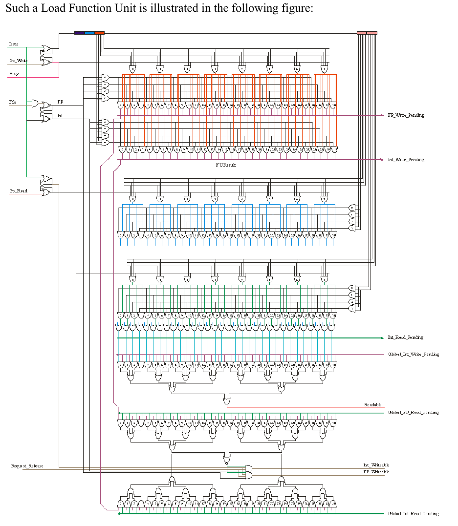
the LOAD Function unit *does* have (and selects from) FP and INT (only one at a time, obviously), where the diagram assumes (reasonably, this being RISC) that the FP regnums and INT regnums from the instruction are in the same bitspace.so from the diagram as-is, my concern was that the regfile selector (marked "FILE" in the attached) would cause SR-Latch instability when "File" is ASSERTED. another potential way to alleviate those concerns i believe would be with a NOT gate and a 2nd AND gate? (attached small similarly badly-drawn diagram).

Jacob Lifshay
lk...@lkcl.net
>
> This design style is deprecated nowadays, along with valves and uni-junction
lk...@lkcl.net
lk...@lkcl.net
>
> The reasons why things were done in a certain way in the
lkcl
> What we know is that we have a Load or a Store being issued, and that there is a signal (FILE)
> that is going to tell us if it is FP (FILE=0) or INT (FILE=1). The memory reference has to target
> one file or the other. The logic I show will assert INT after 2 gates of delay of FP after 1 gate of
> delay (in the SR-flop). Your added logic does not harm, but I don't see it adding good, either.
>
> Also Note: FILE is only used if ISSUE is asserted.
yes, it's asserting the selector AND gates through the other SRLatch
(the one with Go_Write in it).
On Tuesday, May 7, 2019 at 9:31:07 AM UTC+1, lkcl wrote:
soOoo... the instability that would normally occur by driving S and R simultaneously does not occur.... because there is a 2-gate latency in the AND gate. with the "Set" wire simultaneously going into *both* the Set *and* through the 2 gates of AND, it is a physical impossibility for Set and Reset to be asserted at precisely and exactly the same time.that's.... horrendously obscure, efficient and elegant, all at the same time.

lkcl
Hi Mitch,
Ok so I have implemented the gate diagrams to what I believe is a reasonably accurate degree, connected them up with a simple 2 op combinatorial ALU, and some preliminary instructions actually execute and do something (something right, that is)
What I found is as follows:
* the combinatorial nature of the continuous scoreboard causes the simulator to freak out and lock up under certain circumstances.
* this turns out to be related to how SR Latches can't correctly be simulated by nmigen (can't be identified as register-like, nmigen relying on combinatorial blocks being directed acyclic graphs connected only through - separated by - synchronous blocks using DFFs)
* the removal of write-through capability on the register file stops one of the loops (and interestingly still allows ALU operations to proceed combinatorially on the same clock)
* a second loop was tracked down to the "readable" vectors that go into the Issue Unit. this detected when the destination register is also one of the source registers. confusion arose initially as the write thru was *also* causing lockup.
* allowing the "readable" vector to be sync-delayed by 1 clock cuts one of the cyclic points in the combinatorial loop.
* a third point has yet to be tracked down, shown up by throwing random instructions at the engine. i believe it is when a destination reg is used as both a src and dest in a subsequent instruction, this still has to be confirmed and tracked down.
The exercise has allowed me to identify that I had not noticed in all prior readings that the latter stage augmentations, the Continuous Function Units which produce RD/WR vectors, and associated Issue Unit, actually *replace* the 6600 FU - FU Matrix and the secondary FU - Regs Matrix (aka an unary variant of the 1D 6600 Q Table).
This being justifiable by a significant reduction in gate count (16k gates down from 48k).
The issue that I have is, in the continuous (lower gate count) version, I can't identify what constitutes the Q Table (or a variant of it), and that is a crucial thing that provided register renaming, which as you know I plan to extend with historical entries and thus implement precise register renaming.
Can't do that if I can't find it :)
What's the scoop, here?
L.
lkcl
On Thu, May 9, 2019 at 5:05 PM Mitchalsup <mitch...@aol.com> wrote:
>
> You can replace the SR-flops with JK-flops; or D-flops since the logic is so simple.
i quite like the SR-flops, enough to have pseudo-implemented them as a hybrid sync/combinatorial... something. if S, an internal register is set and a combinatorial-output set. else if R, the internal register is cleared and the output also cleared. else, the register is combinatorially output. it seems to work well, and yosys, fascinatingly, turns it into a DFF with 2 MUX gates.
> > * the removal of write-through capability on the register file stops one of the
> A layer of forwarding should alleviate this.
> The write enables that FU to assert Readable.
>
> Q is the logic that connects "I write this register" with "I read this register" such that all prior
> reads can occur before the write (WAR).
> <attempting> writer of the newer value to that register. So Q is where you find the Readables
> NANDing the writables.
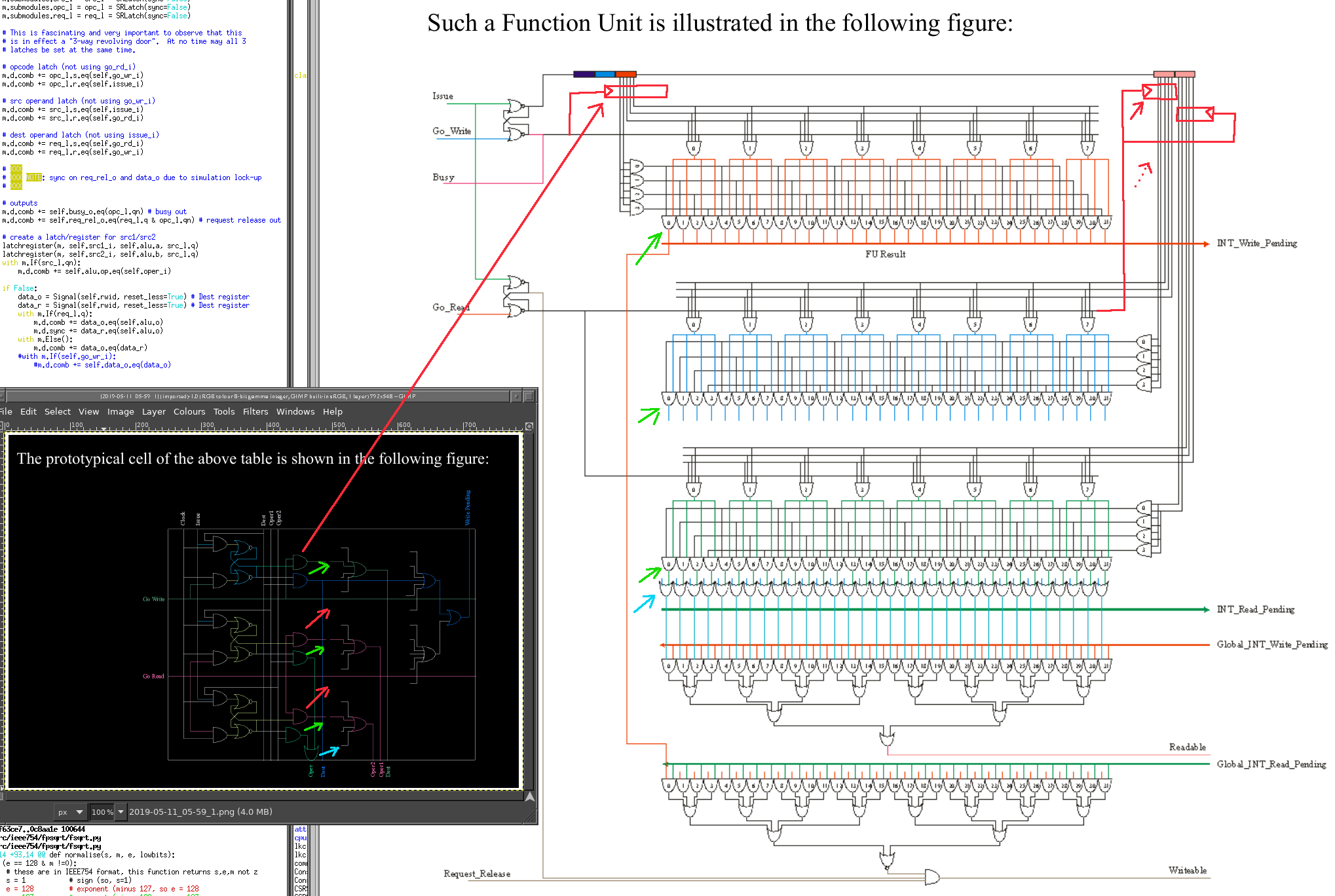
lkcl
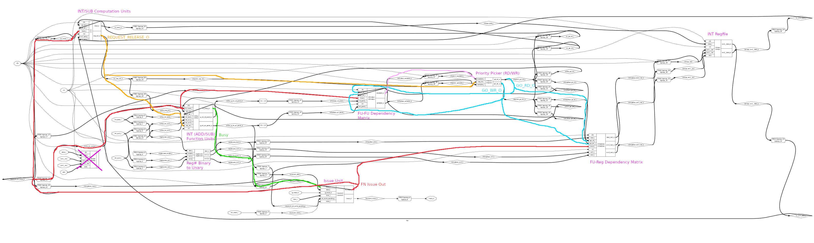
ok, so let's trace it through. the Readables <0:31> and Writables <0:31> all go to the multiple "Priority Pickers", to create one and only one Go_Read and Go_Write per picker (there are 8 pickers)
[this being the way to ensure that, at the Register File, there's no contention for Register File ports.yes want more instructions to be executed simultaneously? add more ports and make sure that a corresponding "Priority Picker" is also added.. *and* more Function Units to feed it].right
so, (see 2nd diagram, p34) the FUs (after routing through Priority Picker(s)) have the Go_Read and Go_Write vectors connected directly to the Register File, which is *no longer an SRAM*, it's an array of DFFs with an array of individual REn/WEn lines... that happen to be exactly and precisely... the Go_Read / Go_Write vectors. Yep, everything is timed from the pickers.in this 2nd diagram, what was formerly two separate matrices, one FU-FU and one FU-Reg, they're now *combined*, replaced with an array of FUs that create FU RD/Write "vectors" (so it is still effectively an FU-Reg Matrix). probably, I haven't given this any thought for over a decade.
this would *tend* to suggest that Q is inside the (new) FU... except that it's not.
what i believe i am looking for is the vertical unary array of flip-flops (one per register), which are illustrated in section 10.5 p24, those being the equivalent of Q table entries (see 3rd attachment, "To a great first order this arrangement is equivalent to the [FU-Reg] Dependency Matrix") This should be the middle figure in chapter 10 on page 25 it is amalgamating the write waits of the figure above.
this unary array per FU (or, in the case of the original 6600, binary-representations aka "just the Destination Reg #") is i believe *missing* from the Continuous Scoreboard Function Units described in section 11.4.8. When I did this (a decade ago) I argued this point until I realized it was already being covered by existing logic. I can't put my finger on exactly where. But you WILL stumble across it.
annotated in red is a latch on the incoming "Dest Reg #" which i *believe*, if added in (along with associated circuitry for detecting when it should be set / reset), would give the register-renaming capability.
Yes.
honestly though i am slightly lost, and may have to go back to the dual Matrices version (independent FU-FU and FU-Reg), which would be quite annoying as it would mean having to work out how to add the "Shadowing" and a few other things besides.Don't give up, you are almost there.
lkcl
it occurred to me overnight that the whole thing works because of the three-way revolving door between issue, read and write [those three being impossible to assert all at the same time].
This is the key, three latches in a row to prevent a run-ahead situation.
any one Function Unit may respond to "issue" on one cycle, then it may respond to "Go_Read" on another subsequent cycle, then "Go_Write" on another. there *may* be clock delays in between.
Right, notice the reuse of a FU has a minimum of a 3 cycle delay.
that these are missing from the control machine on p38 sect 11.4.8 is prooobably why i had to do one issue every 3 clock cycles (and add some sync-latches to pass the information through). one clock for issue, one for read, one for write.
If you are trying to re-use a single FU then you are correct.
If you are not trying to re-use a single FU there should not be a problem in issuing on back to back decode cycles.
with apologies for the large resolution/size of the attached, it shows the FU-Reg Dependency Cell side-by-side with the Function Unit. The only request I have WRT size is to do them in *.jpg
You may be missing a piece of perspective. Imagine that the FUs are close to the issue section ofthe DECODER. and imaging that the CUs are a bus distance away from the issue section. The FUs are clocked at one edge, the CUs are clocked at the successive edge allowing the BUS to be 1clock long.
So the FUs are driving SB logic while the CU are driving computational logic. The FUs always running 1 clock ahead of the corresponding CU.
As long as you don't get a WAW and you don't run out of FUs, you should be able to issue at your hearts content.
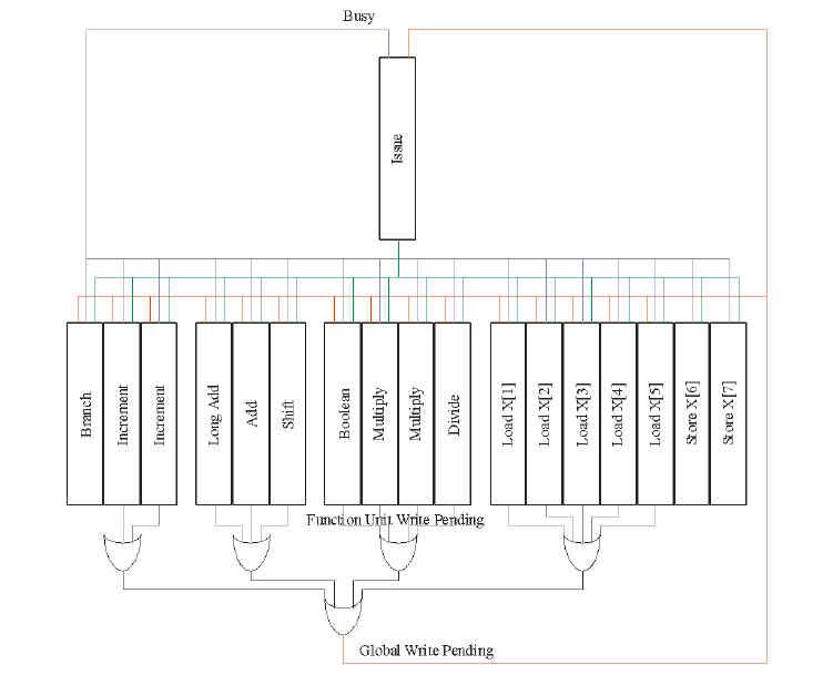
* latched-registers are in red on the Function Unit dest/oper1/oper2 Register #s. these are latched in on "Issue" (assume registers are clock-latched).
Maybe I am missing something::I was using the decoder enables to enable/disable the assertions onto the local XXX_Pending busses which get ORed onto the Global versions.
Once a Go_Read_FU is asserted, the read reservation are removed, locally first, then transitively to global.
Once Go_Write is asserted, the same happens with the Write_Pending signals.
These decoder enables were driven directly from the SR-flops directly from the GO_XXX pickers.So as long as the FU is not re-used faster than 3 cycles, there is time for all this to transpire.
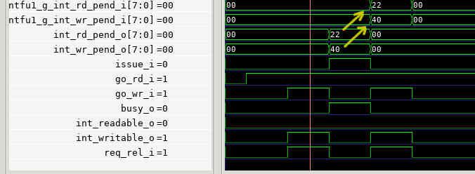
So, are you seeing that Global_INT_Read_Pending is longer than 2 gate delays after INT_Read_Pending? And the same for *Write*?
Let me ask you a few questions::1) How long after Issue_INT does INT_Read+Pending get asserted?
2) How long after Issue_INT does INT_Write_Pending get asserted?
3) How long after Global_INT_Read_Pending does Readable get asserted?
4) How long after Go_Read does INT_Read_Pending get deasserted?
5) How long after Go_Read does Request_Release get asserted?
6) And are the pickers at the end of a clock cycle so that the output of the pickers drives the whole next clock from a read Flip-Flop?
It might be appropriate at this time for you to draw your own schematic.....
lkcl
lkcl
lkcl
lkcl
hi folks, as this was getting a little long, the discussion has migrated here, for anyone who is interested in out-of-order precise designs (that do not require CAMs):as of this afternoon, a demo test 4x4 suite of ALUs works successfully with random instruction allocations avoiding both RaW and WaR hazards, as long as a src register is not used as the destination in any one given instruction. this creates a dependency loop (a RaW *and* WaR hazard) that clearly cannot ever be resolved, and is the current high priority active investigation.
a second bug under investigation is WaW hazards, which, in the 6600 design, are avoided by stalling issue: this is planned to be done through the same mechanism as precise exceptions and branch speculation: prevent write commit until the WaW hazard danger is cleared.
lkcl
the next phases will include adding LD/ST Function Units, branch speculation / cancellation, precise exceptions and more.