FPGA (again) and interfacing advice

Les Bird

Dan Emrick
Les Bird
Les Bird
Les Bird

Douglas Miller
My gut-reaction would be that the FPGA can't drive the H8 adequately anyway, the same way the 8080 chipset couldn't. Seems to me you need buffers of some sort (inverting at that, unless the FPGA is programmed for it), and so level-shifters are the right choice it would seem. The data bus will require bi-directional. There seems to be lots of them out there, although bidirectional are probably harder to find. But, I think you should be able to find actual ICs to that, rather than BOBs with discrete parts.
--
You received this message because you are subscribed to the Google Groups "SEBHC" group.
To unsubscribe from this group and stop receiving emails from it, send an email to sebhc+un...@googlegroups.com.
To view this discussion on the web visit https://groups.google.com/d/msgid/sebhc/f1188afd-34f5-4679-be2f-1b4ee9f8b0e4n%40googlegroups.com.

norberto.collado koyado.com
Sent: Wednesday, December 14, 2022 3:19:52 PM
To: SEBHC <se...@googlegroups.com>
Subject: [sebhc] Re: FPGA (again) and interfacing advice

Dave McGuire
> My gut-reaction would be that the FPGA can't drive the H8 adequately
> anyway, the same way the 8080 chipset couldn't. Seems to me you need
> buffers of some sort (inverting at that, unless the FPGA is programmed
> for it), and so level-shifters are the right choice it would seem. The
> data bus will require bi-directional. There seems to be lots of them out
> there, although bidirectional are probably harder to find. But, I think
> you should be able to find actual ICs to that, rather than BOBs with
> discrete parts.
many designs; they've performed very well for me.
-Dave
--
Dave McGuire, AK4HZ
New Kensington, PA
Douglas Miller
level-translators suffice for bus drivers, too... or does one still need
something to drive the H8 bus? The data sheet is making my eyes glaze
over, but I don't see anything indicating a significant current capability.
Dave McGuire
Oooh. Yes, that's a good point. I've never used them as bus
drivers, only as interfaces between different logic families.
-Dave
Les Bird
Les Bird
Douglas Miller
I believe that each "translator" has a current limit, and if I'm reading the datasheet correctly it is pretty small. There is a fair amount of current needed (by comparison) to drive multiple TTL inputs in the various H8 boards. Also, just the length of the traces requires some current to drive the signals quickly to "1" or "0". I believe these translators are meant for direct, proximal, connection of two low-power devices.
--
You received this message because you are subscribed to the Google Groups "SEBHC" group.
To unsubscribe from this group and stop receiving emails from it, send an email to sebhc+un...@googlegroups.com.
To view this discussion on the web visit https://groups.google.com/d/msgid/sebhc/612ced3f-aaac-46cb-a43c-1b36f51c1463n%40googlegroups.com.
Les Bird
Dan Emrick
Dave McGuire
Yes, it's only a logic level translator. No substantial drive
capability.
-Dave
> --
> You received this message because you are subscribed to the Google
> Groups "SEBHC" group.
> To unsubscribe from this group and stop receiving emails from it, send
> an email to sebhc+un...@googlegroups.com

Peter Higgins
Peter Higgins
Les Bird
--
You received this message because you are subscribed to the Google Groups "SEBHC" group.
To unsubscribe from this group and stop receiving emails from it, send an email to sebhc+un...@googlegroups.com.
To view this discussion on the web visit https://groups.google.com/d/msgid/sebhc/f05866f2-8753-4550-a1d0-e9e58859b590n%40googlegroups.com.
Les Bird
norberto.collado koyado.com
Congratulations Les on your first H8 FPGA board. Nicely done!
Norberto
From: se...@googlegroups.com <se...@googlegroups.com>
On Behalf Of Les Bird
Sent: Thursday, December 29, 2022 6:38 AM
To: SEBHC <se...@googlegroups.com>
Subject: Re: [sebhc] Re: FPGA (again) and interfacing advice
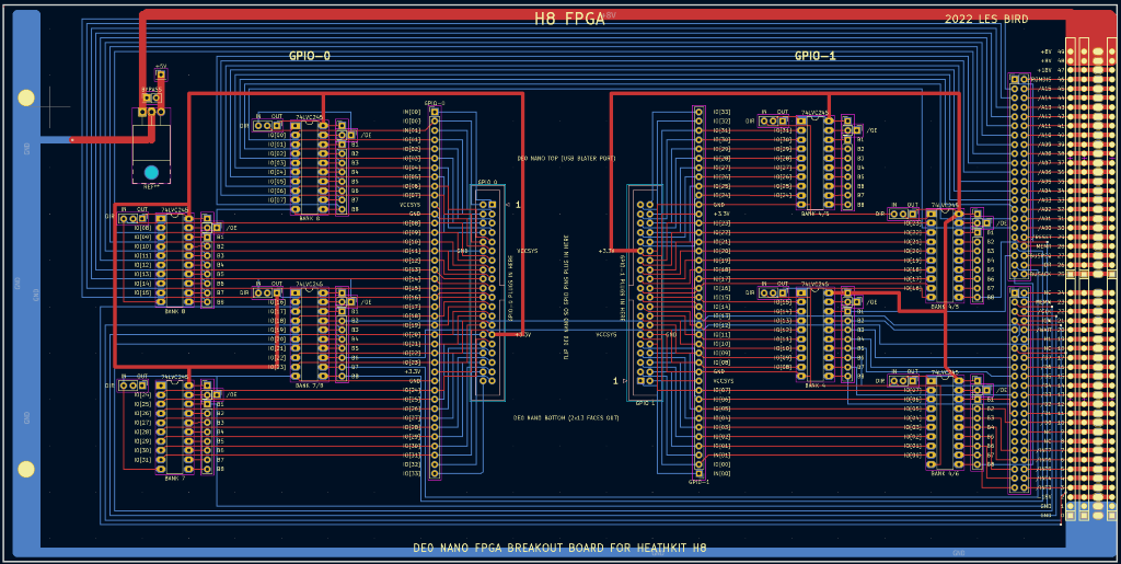
Well I sent my first PCB to JLCPCB (thanks Scott!). It's been a while since I made a PCB. Basically a DE0-NANO FPGA breakout board for the H8. $40 including shipping (with $10 new customer discount) for 5 boards. Pretty good prices. I'm using 74LVC245's to interface to the H8 BUSS and for each chip you can set a jumper for it to be incoming or outgoing (the LVC245s are bidirectional). Once you decide which pins on the FPGA are incoming you can then set the jumper on the 245 to match, same for outgoing. The default configuration for the board is for all GPIO-0 pins to be outgoing and all GPIO-1 pins to be incoming. I've wired up an optional configuration for the board to act as a CPU board replacement - the jumpers on the right side of the board by the edge connectors, if they are all jumpered then this configuration (CPU board) will be active. If not jumpered then you can wirewrap you're own setup from the outputs of the LVC245s to the pin headers at the edge connectors so this board can be configured to do just about anything. You can also decide to not use any of the LVC245s and work directly from the GPIO breakout pins.
And when I say it's configured as a CPU board if you jumper the right side I mean I have a default set of GPIO pins wired to all the appropriate pins on the H8 buss to look like a CPU board. The Google Sheet linked below has the current FPGA to H8 BUSS mapping:
https://docs.google.com/spreadsheets/d/1-CI0nU_hhu6U5jDEmocSR6qhjhgz6WzZZCHjXEHm33Y/edit?usp=sharing
This is V1.0 of the FPGA breakout board so we'll see if it works. It's all just a prototype right now.
Les

On Friday, December 16, 2022 at 9:26:17 AM UTC-7 Les Bird wrote:
Good information Peter, thank you.
Les
On Thu, Dec 15, 2022 at 10:07 AM Peter Higgins <higgin...@gmail.com> wrote:
Altera Cyclone-based FPGAs have been the basis of several projects for the S100 bus:
Level translation (5V to 3.3V) is typically performed using the 74LVC245, which is powered by 3.3V, has a 3.3V drive output, but is designed to accept input from 5V logic.
You will see the S100 bus designs I linked to above also use the 74LVC245 for 3.3V to 5V logic translation and driving the bus. These designs power the 74LVC245 with 5V instead of 3V (which is above typical but within max specifications) however a standard 74LS245 works just as well since the logic "high" level produced by the 3.3V FPGA adequately meets the minimum logic high level for an LSTTL device.
On Wednesday, December 14, 2022 at 12:30:48 PM UTC-8 Les Bird wrote:
Hi all,
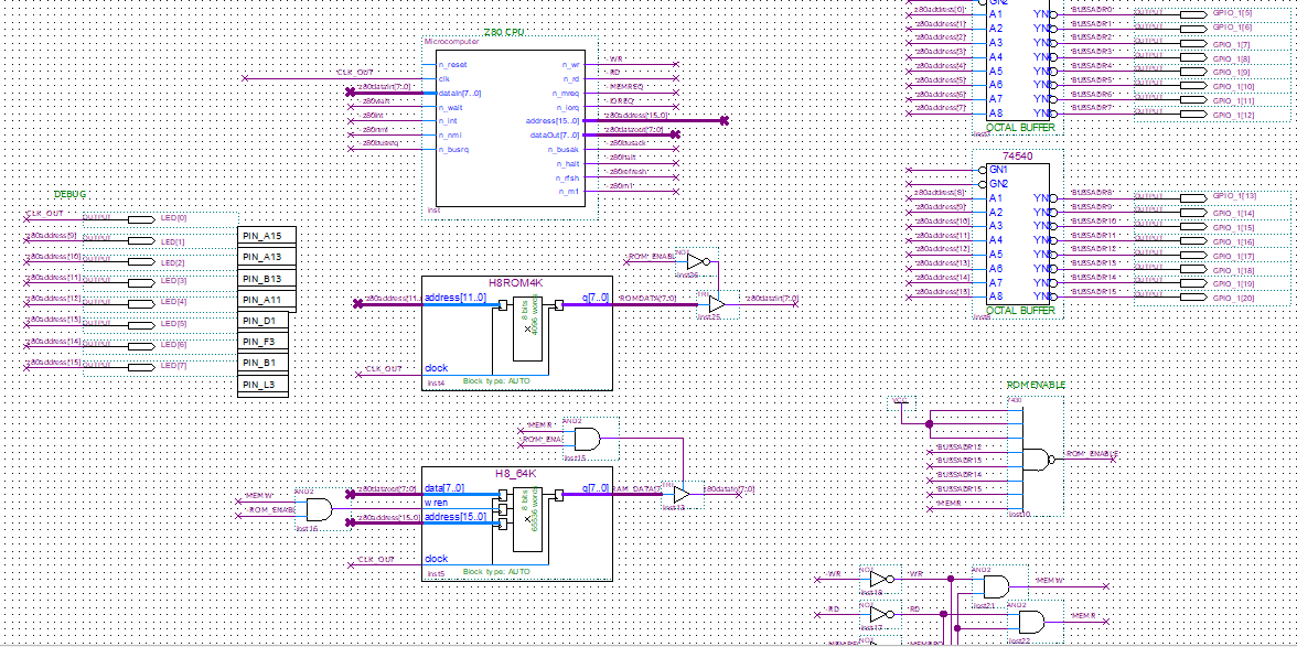
A while back I brought up the topic of building a H8 CPU on a FPGA. Well, I'm back at it again. I discovered recently (actually Rob Doyle mentioned this in our last conversation) that I can actually "program" the FPGA using BDF files (like schematics) which I understand a lot better than the verilog language. For those who are curious you can layout a schematic and it will be converted to verilog and then the resulting compiled code uploaded to the FPGA. (see photo).
I have a question for the experts regarding interfacing to the H8 buss.
The H8 buss is +5V TTL. I have a DE0-NANO FPGA board with GPIO pins. My plan is to "plug" the FPGA into the buss by wiring up a harness from the GPIO bins to two 25-pin connectors that plug into the H8 buss. The FPGA board has 3.3V on the pins. Do I need to do anything special in between the GPIO pins and the H8 buss? I looked online but can't find a solid answer - some say it'll work fine, some say there potentially needs to be some conversion circuitry. Not sure which way to go.
Also, do we have a good schematic for the HA-8-6 Z80 board? The one I have on SEBHC is broken up into several PDFs. Wondering if we have one that is one piece so it's easier to read or maybe if someone can stitch the schematic together from SEBHC.
There are some real benefits to putting the Z80 CPU on a FPGA. First, we'll never have to worry about parts that are going obsolete and no longer available. Second, we can make tweaks to the board and simply upload the new design to the FPGA without having to get prototype boards made, debug, and then get final boards from the PCB house. Third, a LOT fewer parts that can go bad. Fourth, substantial cost savings - aside from what I mentioned earlier about no PCBs needed a DE0-NANO cost $120 from MOUSER - no parts to source - and it can be reprogrammed with new functionality/features at anytime.
Now that I learned about laying out schematics on the FPGA this has been a very enjoyable experience for me so far.
Les
--
You received this message because you are subscribed to the Google Groups "SEBHC" group.
To unsubscribe from this group and stop receiving emails from it, send an email to sebhc+un...@googlegroups.com.To view this discussion on the web visit https://groups.google.com/d/msgid/sebhc/f05866f2-8753-4550-a1d0-e9e58859b590n%40googlegroups.com.
--
You received this message because you are subscribed to the Google Groups "SEBHC" group.
To unsubscribe from this group and stop receiving emails from it, send an email to
sebhc+un...@googlegroups.com.
To view this discussion on the web visit https://groups.google.com/d/msgid/sebhc/aac97eb8-3fd8-41ea-a1f5-f570627187cen%40googlegroups.com.
norberto.collado koyado.com
Also your layouts are so beautiful when compare to the ones I do. 😊
To view this discussion on the web visit https://groups.google.com/d/msgid/sebhc/SN6PR01MB38553A9953FA7EE820C516B1F7F39%40SN6PR01MB3855.prod.exchangelabs.com.
Les Bird

Joseph Travis
To view this discussion on the web visit https://groups.google.com/d/msgid/sebhc/ff54414d-d32a-424d-890b-d611bfe9ffcfn%40googlegroups.com.
norberto.collado koyado.com
I noticed that, but for this first board pass should be fine. You can do 1-per IC or 1-per three IC’s. Please use 0.1uf as all my new boards uses this cap and we have a lot in stock to build out new boards.
To view this discussion on the web visit https://groups.google.com/d/msgid/sebhc/ff54414d-d32a-424d-890b-d611bfe9ffcfn%40googlegroups.com.
Les Bird
norberto.collado koyado.com
Very nice Les! Thank you!
😊
From: se...@googlegroups.com <se...@googlegroups.com>
On Behalf Of Les Bird
Sent: Friday, January 27, 2023 7:29 PM
To: SEBHC <se...@googlegroups.com>
Subject: Re: [sebhc] Re: FPGA (again) and interfacing advice
Hi all,
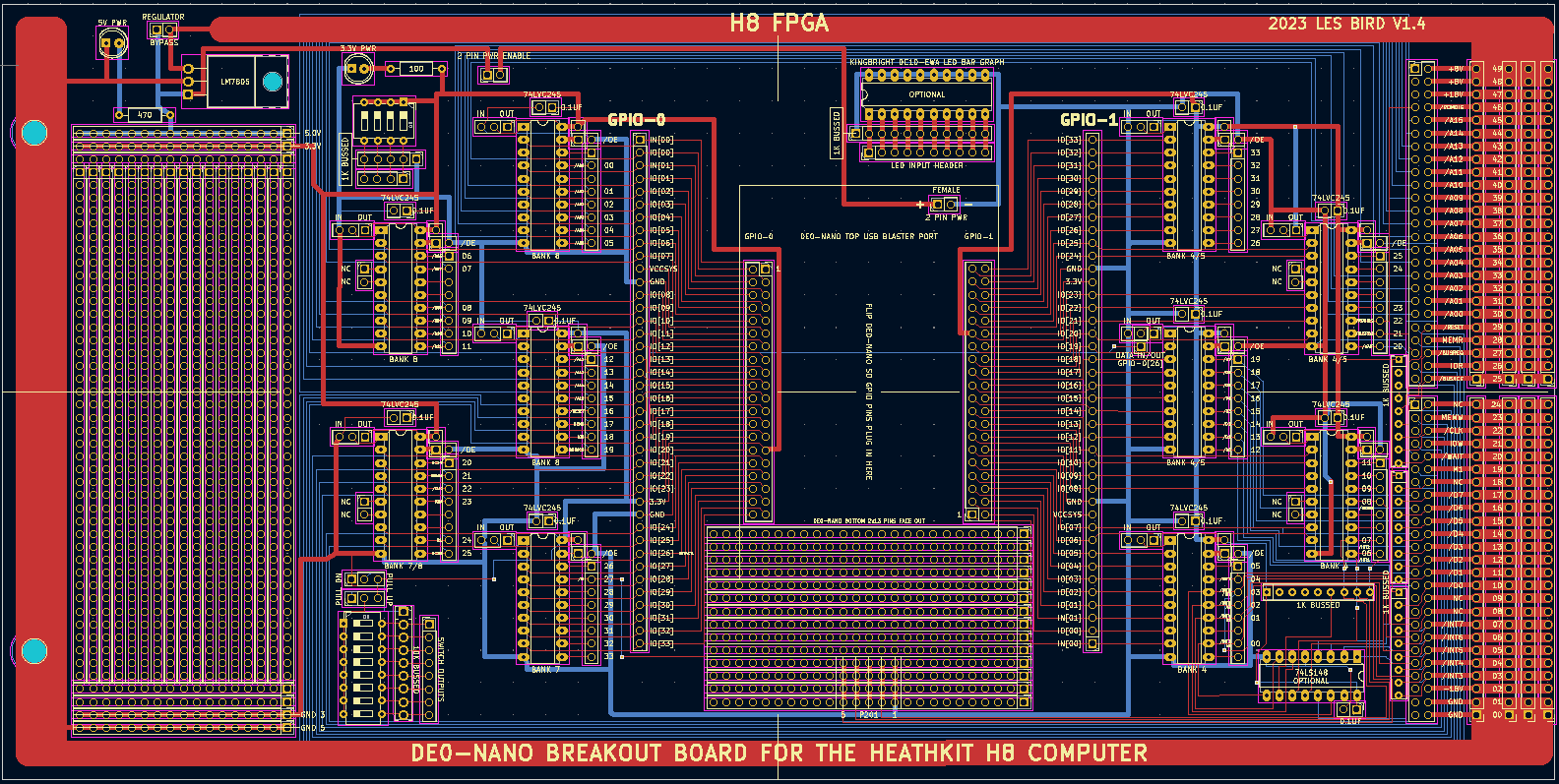
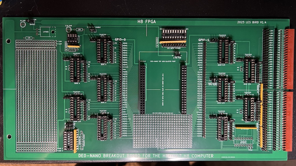
Just a quick update. My FPGA breakout board is at V1.4 now currently in production at JLCPCB. It's come a long way. I added the filter caps and some prototype areas along with pull up resistors and an optional spot for a 74LS148 interrupt decoder. If I ever get the FPGA Z80 CPU board working then that should open up support for the H37 controller. I've also added 2 sets of dip switches (4 and 8 switch) and an optional spot for a LED bar graph at the top for debugging or whatever.
Currently I'm just trying to get the FPGA Z80 CPU to work with the front panel. I think it's close but it's not there yet. The ROM and RAM are integrated into the FPGA design and with the DE0-NANO there's even 32mb of SDRAM that I hope to tap into in the future. Will keep you all posted as I make more progress with it.
The 74LVC245s work well as an interface to the H8 buss. I'm getting good signals to the buss (3.3v to 5.0v) measured on the front panel and from the buss (5.0v to 3.3v).
V1.4 layout:

To view this discussion on the web visit https://groups.google.com/d/msgid/sebhc/ed3cc1ac-f782-4282-b14e-659645647ff5n%40googlegroups.com.

Mark Garlanger
To view this discussion on the web visit https://groups.google.com/d/msgid/sebhc/SN6PR01MB38558749D72EF1C61B84E5D9F7CD9%40SN6PR01MB3855.prod.exchangelabs.com.
Les Bird
Les Bird
norberto.collado koyado.com
Les Bird
norberto.collado koyado.com
norberto.collado koyado.com
Sent: Monday, January 30, 2023 1:09:51 PM
To: se...@googlegroups.com <se...@googlegroups.com>
Peter Higgins
norberto.collado koyado.com
Very nice and thank you!
Norberto
From:
se...@googlegroups.com <se...@googlegroups.com> on behalf of Peter Higgins <higgin...@gmail.com>
Date: Monday, January 30, 2023 at 2:39 PM
To: SEBHC <se...@googlegroups.com>
Subject: Re: [sebhc] Re: FPGA (again) and interfacing advice
--
You received this message because you are subscribed to the Google Groups "SEBHC" group.
To unsubscribe from this group and stop receiving emails from it, send an email to
sebhc+un...@googlegroups.com.
To view this discussion on the web visit https://groups.google.com/d/msgid/sebhc/b7b957dd-1254-4a2c-884d-7fd5a82f7cc5n%40googlegroups.com.
Les Bird


norberto.collado koyado.com
WOW, Les! I’m impressed.
Great job in getting this new design working. Congratulations.
Norberto
From: se...@googlegroups.com <se...@googlegroups.com>
On Behalf Of Les Bird
Sent: Friday, February 3, 2023 6:46 AM
To: SEBHC <se...@googlegroups.com>
Subject: Re: [sebhc] Re: FPGA (again) and interfacing advice
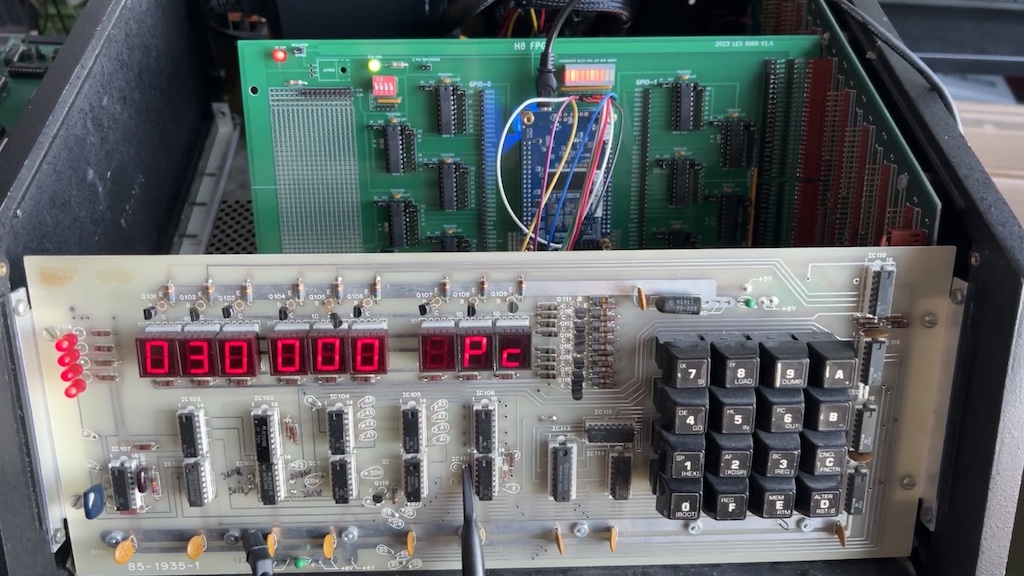
Very excited to report that the FPGA Z80 CPU board is starting to show some life! :)
I'm using the PAM8GO ROM for starters and then I'll move on to XCON8 once I get PAM8GO working.
It is not reading the keypad though so I'll have to debug that but I'm excited to see that it is communicating with the front panel and displaying the PC address on the LEDs. I'm getting clean INT1's from the front panel finally (previously I was not able to get any INT1's) so this is a big step forward.

On Monday, January 30, 2023 at 10:13:34 PM UTC-7 Norby wrote:
Very nice and thank you!
Norberto
From: se...@googlegroups.com <se...@googlegroups.com> on behalf of Peter Higgins <higgin...@gmail.com>
Date: Monday, January 30, 2023 at 2:39 PM
To: SEBHC <se...@googlegroups.com>
Subject: Re: [sebhc] Re: FPGA (again) and interfacing adviceThis is the DE0-Nano board:
Available from multiple vendors including Digi-Key and Mouser for $115.
One of the contributors to the S100Computers Google Group has recently developed an FPGA development module for use with future S100 board designs. It uses the Efinix T35 FPGA core (with 180K of its own embedded RAM) and 64Mx16 of DDR3 RAM onboard. It costs under $100.
On Monday, January 30, 2023 at 1:11:16 PM UTC-8 Norby wrote:
Just curious how much the FPGA board costs with such RAM capacity?
--
You received this message because you are subscribed to the Google Groups "SEBHC" group.
To unsubscribe from this group and stop receiving emails from it, send an email to sebhc+un...@googlegroups.com.To view this discussion on the web visit https://groups.google.com/d/msgid/sebhc/b7b957dd-1254-4a2c-884d-7fd5a82f7cc5n%40googlegroups.com.
--
You received this message because you are subscribed to the Google Groups "SEBHC" group.
To unsubscribe from this group and stop receiving emails from it, send an email to
sebhc+un...@googlegroups.com.
To view this discussion on the web visit https://groups.google.com/d/msgid/sebhc/b15084e1-c358-4127-bc27-5e17dbdb49e7n%40googlegroups.com.

Richard Davis Jr.
To view this discussion on the web visit https://groups.google.com/d/msgid/sebhc/b15084e1-c358-4127-bc27-5e17dbdb49e7n%40googlegroups.com.
Les Bird
norberto.collado koyado.com
As I use Quartus a lot @Intel to flash the Server FPGA’s/CPLD, just let me know how I can help.
I have my own USB Blaster II to program FPGA’s as I was planning to develop a board to learn FPGA, but never got to it.
Which one you are using to update the FPGA?
Norberto
From: se...@googlegroups.com <se...@googlegroups.com>
On Behalf Of Les Bird
Sent: Friday, February 3, 2023 10:00 AM
To: SEBHC <se...@googlegroups.com>
Subject: Re: [sebhc] Re: FPGA (again) and interfacing advice
Thanks Norby and Rick!
I almost gave up on this project. Quartus (the FPGA design software) is not the easiest piece of software to use and seems quite buggy but after pushing through a couple of weird Quartus bugs I was able to make some good progress with the FPGA layout design. Also the new 1.4 PCB fixed a couple issues I was having with the earlier boards. I received the new boards yesterday and after building it and plugging it in it immediately booted to the front panel so that was very exciting to see. Months of work is starting to pay off finally. Still lots to do but this is good progress.
Les
On Friday, February 3, 2023 at 9:23:20 AM UTC-7 rickdav...@gmail.com wrote:
Les,
This is really neat!
Congrats.
Rick
On Fri, Feb 3, 2023 at 9:46 AM Les Bird <lesb...@gmail.com> wrote:
Very excited to report that the FPGA Z80 CPU board is starting to show some life! :)
I'm using the PAM8GO ROM for starters and then I'll move on to XCON8 once I get PAM8GO working.
It is not reading the keypad though so I'll have to debug that but I'm excited to see that it is communicating with the front panel and displaying the PC address on the LEDs. I'm getting clean INT1's from the front panel finally (previously I was not able to get any INT1's) so this is a big step forward.

On Monday, January 30, 2023 at 10:13:34 PM UTC-7 Norby wrote:
Very nice and thank you!
Norberto
From: se...@googlegroups.com <se...@googlegroups.com> on behalf of Peter Higgins <higgin...@gmail.com>
Date: Monday, January 30, 2023 at 2:39 PM
To: SEBHC <se...@googlegroups.com>
Subject: Re: [sebhc] Re: FPGA (again) and interfacing adviceThis is the DE0-Nano board:
Available from multiple vendors including Digi-Key and Mouser for $115.
One of the contributors to the S100Computers Google Group has recently developed an FPGA development module for use with future S100 board designs. It uses the Efinix T35 FPGA core (with 180K of its own embedded RAM) and 64Mx16 of DDR3 RAM onboard. It costs under $100.
On Monday, January 30, 2023 at 1:11:16 PM UTC-8 Norby wrote:
Just curious how much the FPGA board costs with such RAM capacity?
--
You received this message because you are subscribed to the Google Groups "SEBHC" group.
To unsubscribe from this group and stop receiving emails from it, send an email to sebhc+un...@googlegroups.com.To view this discussion on the web visit https://groups.google.com/d/msgid/sebhc/b7b957dd-1254-4a2c-884d-7fd5a82f7cc5n%40googlegroups.com.
--
You received this message because you are subscribed to the Google Groups "SEBHC" group.
To unsubscribe from this group and stop receiving emails from it, send an email to sebhc+un...@googlegroups.com.
To view this discussion on the web visit https://groups.google.com/d/msgid/sebhc/b15084e1-c358-4127-bc27-5e17dbdb49e7n%40googlegroups.com.
--
You received this message because you are subscribed to the Google Groups "SEBHC" group.
To unsubscribe from this group and stop receiving emails from it, send an email to
sebhc+un...@googlegroups.com.
To view this discussion on the web visit https://groups.google.com/d/msgid/sebhc/52e7d2d9-a361-490e-a0c0-75e83cf49467n%40googlegroups.com.
Les Bird
norberto.collado koyado.com
Sent: Friday, February 3, 2023 1:10:45 PM
Peter Higgins

Frank Madison
norberto.collado koyado.com
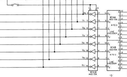
Yes, you are correct. The old FP keyboard inputs to the IC are floating as they are TTL, internally they will decode as a “1” level. A 74HCT will decode internally as a “0” and it won’t work. I fixed this on the new front panel, so you can use either IC 74LS or 74HCT. Also, same issue reported by Scott on the H17 74LS30 and fixed that as well as he was using the 74HCT family.
In Les case, based on the schematic, it could be his FPGA having issues reading on port 360Q that enables pin 1,19 on IC113, as long he is using the 74LS family for the line encoder IC.
As the FP LEDs are operational the FPGA writes are working.
Norberto
From: se...@googlegroups.com <se...@googlegroups.com>
On Behalf Of Frank Madison
Sent: Friday, February 3, 2023 10:06 PM
To: se...@googlegroups.com
Subject: Re: [sebhc] Re: FPGA (again) and interfacing advice
Les,
In case you have not yet figured out your keyboard problem, let me mention a problem I once found that may provide guidance. The keys on the front panel do not have pull-downs. They rely on 74xx TTL having current-mode inputs. I tried using 74HCxx to replace a keyboard IC, and it did not work. You may have to program your FPGA inputs to activate a pull-down resistors if they are available on the device that your are using.
Regards
Frank
Sent: Friday, February 03, 2023 at 7:46 AM
From: "Les Bird" <lesb...@gmail.com>
To: "SEBHC" <se...@googlegroups.com>
Subject: Re: [sebhc] Re: FPGA (again) and interfacing advice
Very excited to report that the FPGA Z80 CPU board is starting to show some life! :)
I'm using the PAM8GO ROM for starters and then I'll move on to XCON8 once I get PAM8GO working.
It is not reading the keypad though so I'll have to debug that but I'm excited to see that it is communicating with the front panel and displaying the PC address on the LEDs. I'm getting clean INT1's from the front panel finally (previously I was not able to get any INT1's) so this is a big step forward.


On Monday, January 30, 2023 at 10:13:34 PM UTC-7 Norby wrote:
Very nice and thank you!
Norberto
From: se...@googlegroups.com <se...@googlegroups.com> on behalf of Peter Higgins <higgin...@gmail.com>
Date: Monday, January 30, 2023 at 2:39 PM
To: SEBHC <se...@googlegroups.com>
Subject: Re: [sebhc] Re: FPGA (again) and interfacing adviceThis is the DE0-Nano board:
Available from multiple vendors including Digi-Key and Mouser for $115.
One of the contributors to the S100Computers Google Group has recently developed an FPGA development module for use with future S100 board designs. It uses the Efinix T35 FPGA core (with 180K of its own embedded RAM) and 64Mx16 of DDR3 RAM onboard. It costs under $100.
On Monday, January 30, 2023 at 1:11:16 PM UTC-8 Norby wrote:
Just curious how much the FPGA board costs with such RAM capacity?
--
You received this message because you are subscribed to the Google Groups "SEBHC" group.
To unsubscribe from this group and stop receiving emails from it, send an email to sebhc+un...@googlegroups.com.To view this discussion on the web visit https://groups.google.com/d/msgid/sebhc/b7b957dd-1254-4a2c-884d-7fd5a82f7cc5n%40googlegroups.com.
--
You received this message because you are subscribed to the Google Groups "SEBHC" group.
To unsubscribe from this group and stop receiving emails from it, send an email to
sebhc+un...@googlegroups.com.
To view this discussion on the web visit
https://groups.google.com/d/msgid/sebhc/b15084e1-c358-4127-bc27-5e17dbdb49e7n%40googlegroups.com.
--
You received this message because you are subscribed to the Google Groups "SEBHC" group.
To unsubscribe from this group and stop receiving emails from it, send an email to
sebhc+un...@googlegroups.com.
To view this discussion on the web visit https://groups.google.com/d/msgid/sebhc/trinity-5b8337cc-3c1e-420e-8124-7012cbbbb5b0-1675490785912%403c-app-mailcom-lxa13.
Les Bird
Les Bird
norberto.collado koyado.com
WOW! Will this be challenging to be able to boot from the H17 board due to the timing constants?
From: se...@googlegroups.com <se...@googlegroups.com>
On Behalf Of Les Bird
Sent: Saturday, February 4, 2023 7:15 AM
To: SEBHC <se...@googlegroups.com>
Subject: Re: [sebhc] Re: FPGA (again) and interfacing advice
Frank,
Thanks for the tip. I did get it working but weirdly enough it was due to the Z80 core not running quick enough. I think the problem was it kept getting interrupted by the 2ms front panel interrupt and wasn't able to poll the keypad quick enough. Here's what I discovered, running the Z80 core at 2.08Mhz would not get any IOR to the front panel or it would get them but on very rare occasions. Once I bumped up the core speed to 4Mhz I started to get some activity on the keypad but it was not reliable. I bumped up to 5Mhz and it worked perfectly. I was getting reliable IOR on the front panel and inputting the "your h8 is up and running" test program worked fine.
I tried a bunch of things to work around this. For example, running the core at 5Mhz and outputting 2Mhz to the BUSS but that didn't work at all.
I think what I'm going to do is change out the core from T80s to maybe the A-Z80 to see if it operates better.
On the front panel I measured 49khz from the M1 line but it should be at a solid 249khz (based on real Z80 card). The INT1 (pin C on front panel) should be at a steady 500hz but I was seeing it bounce around from 420 to 508hz. So it seems like there are different timings when using the T80s core.

On Friday, February 3, 2023 at 11:06:29 PM UTC-7 Frank_M wrote:
Les,
In case you have not yet figured out your keyboard problem, let me mention a problem I once found that may provide guidance. The keys on the front panel do not have pull-downs. They rely on 74xx TTL having current-mode inputs. I tried using 74HCxx to replace a keyboard IC, and it did not work. You may have to program your FPGA inputs to activate a pull-down resistors if they are available on the device that your are using.
To: "SEBHC" <se...@googlegroups.com>
Subject: Re: [sebhc] Re: FPGA (again) and interfacing advice
Very excited to report that the FPGA Z80 CPU board is starting to show some life! :)
I'm using the PAM8GO ROM for starters and then I'll move on to XCON8 once I get PAM8GO working.
It is not reading the keypad though so I'll have to debug that but I'm excited to see that it is communicating with the front panel and displaying the PC address on the LEDs. I'm getting clean INT1's from the front panel finally (previously I was not able to get any INT1's) so this is a big step forward.
On Monday, January 30, 2023 at 10:13:34 PM UTC-7 Norby wrote:
Very nice and thank you!
Norberto
From: se...@googlegroups.com <se...@googlegroups.com> on behalf of Peter Higgins <higgin...@gmail.com>
Date: Monday, January 30, 2023 at 2:39 PM
To: SEBHC <se...@googlegroups.com>
Subject: Re: [sebhc] Re: FPGA (again) and interfacing adviceThis is the DE0-Nano board:
Available from multiple vendors including Digi-Key and Mouser for $115.
One of the contributors to the S100Computers Google Group has recently developed an FPGA development module for use with future S100 board designs. It uses the Efinix T35 FPGA core (with 180K of its own embedded RAM) and 64Mx16 of DDR3 RAM onboard. It costs under $100.
On Monday, January 30, 2023 at 1:11:16 PM UTC-8 Norby wrote:
Just curious how much the FPGA board costs with such RAM capacity?
--
You received this message because you are subscribed to the Google Groups "SEBHC" group.
To unsubscribe from this group and stop receiving emails from it, send an email to sebhc+un...@googlegroups.com.To view this discussion on the web visit https://groups.google.com/d/msgid/sebhc/b7b957dd-1254-4a2c-884d-7fd5a82f7cc5n%40googlegroups.com.
--
You received this message because you are subscribed to the Google Groups "SEBHC" group.
To unsubscribe from this group and stop receiving emails from it, send an email to sebhc+un...@googlegroups.com.
To view this discussion on the web visit https://groups.google.com/d/msgid/sebhc/b15084e1-c358-4127-bc27-5e17dbdb49e7n%40googlegroups.com.
--
You received this message because you are subscribed to the Google Groups "SEBHC" group.
To unsubscribe from this group and stop receiving emails from it, send an email to
sebhc+un...@googlegroups.com.
To view this discussion on the web visit https://groups.google.com/d/msgid/sebhc/a1bb5b0d-48f8-40a1-ab15-74de4473d023n%40googlegroups.com.
Frank Madison
Les Bird
Les Bird
norberto.collado koyado.com
Great Job Les! I always said, nothing like the real hardware. When I did try to emulate the SASI bus with software on my first Z67-IDE controller, it was hard to get the correct timing under software. I was not able to get it run over 4MHz. The instructions, I had to pick the right ones with lower cycle times to maintain the correct timing. I almost spend a year on such controller to get it to work.
Then I decided to use the SASI controller to the job on the Z67-IDE+ and I got it running within weeks. The positive was that it was capable to boot up to 16MHz. Now with the Z180, it makes it easy to maintain such speeds.
Once more time I decided to do SASI under software control on the Z67-SD controller using new and cheaper microcontroller. It failed even to boot consistently at 2MHz. A total failure.
Now the new Z67-SD controller I will use again SASI controller to be able to maintain the necessary throughput.
On your FPGA design is not that easy, but it will take time and effort.
Keep the pictures coming…
Thanks,
Norberto
From: se...@googlegroups.com <se...@googlegroups.com>
On Behalf Of Les Bird
Sent: Tuesday, February 7, 2023 5:48 PM
To: SEBHC <se...@googlegroups.com>
Subject: Re: [sebhc] Re: FPGA (again) and interfacing advice
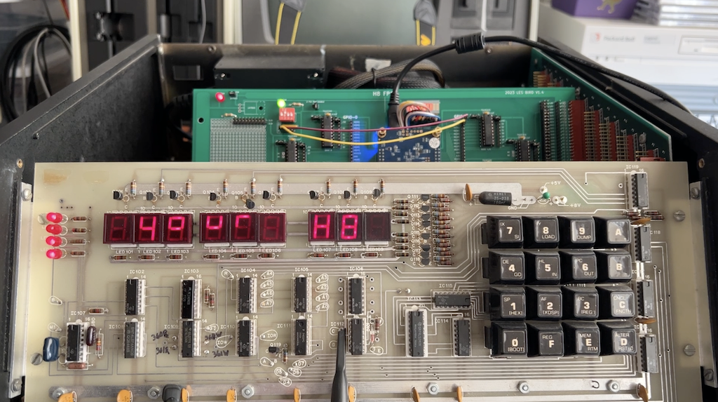
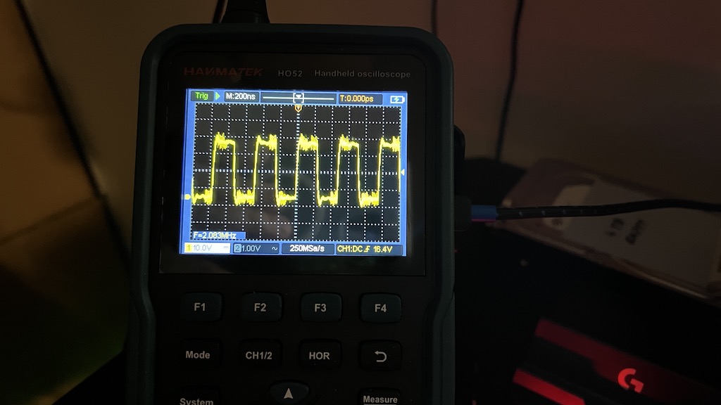
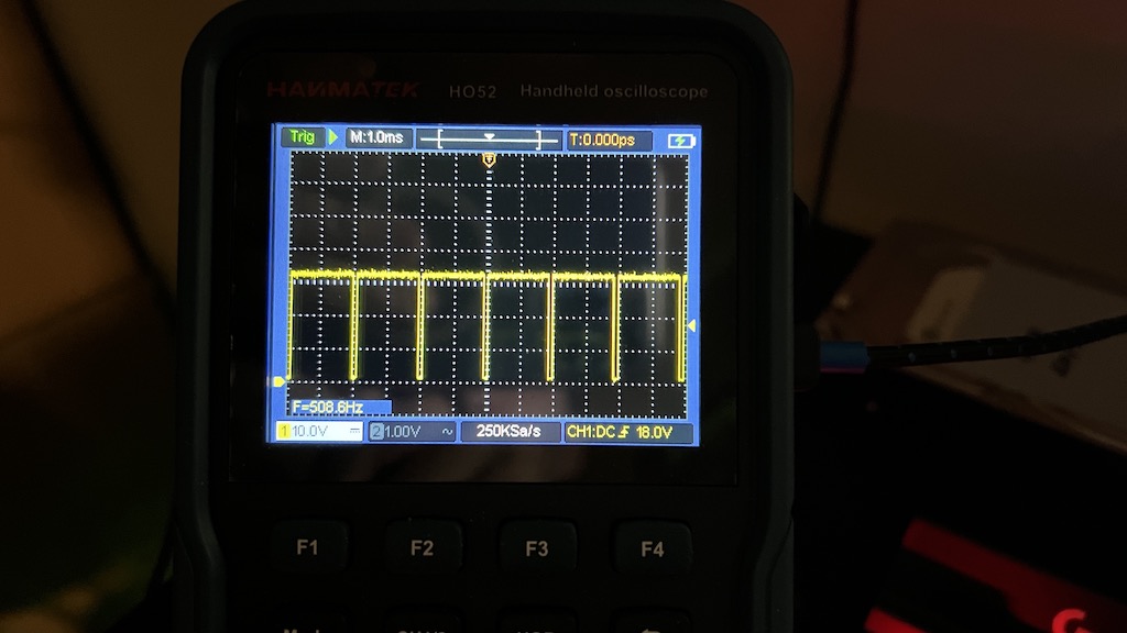
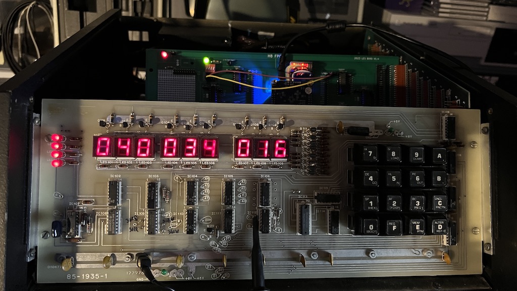
After lots of tuning I've made some good progress with the FPGA Z80 card. As shown in the screen shots I'm getting a solid 508Hz on the 2MS interrupt with the Z80 pushing 2.08MHz to the H8 BUSS and the Z80 core running at 25MHz.. On the M1 line I'm getting 347KHz which is a lot higher then the standard Z80 which is 249KHz. Might need to do some additional tweaking to get it down to where it needs to be. The front panel keypad is working perfectly and the LED display is rock solid.
I still have a lot to do but I'm thrilled with the results so far. It is currently running the 1K PAM8GO ROM.


On Saturday, February 4, 2023 at 8:06:14 PM UTC-7 Frank_M wrote:
Les,
I'm glad to hear that you have the problem figured out. It would be nice if there were a Z80 core that was not only behaviorly the same as the Zilog device, but was electronically the same (providing the same timing).
I've often thought of using programmable logic to combine all the "glue logic" on the H8. Since that logic is mostly combinatorial rather than synchronous, timing would not be an issue.
I've been following your progress. Keep up the good work.
Frank
Sent: Saturday, February 04, 2023 at 8:15 AM
From: "Les Bird" <lesb...@gmail.com>
To: "SEBHC" <se...@googlegroups.com>
Subject: Re: [sebhc] Re: FPGA (again) and interfacing advice
Frank,
Thanks for the tip. I did get it working but weirdly enough it was due to the Z80 core not running quick enough. I think the problem was it kept getting interrupted by the 2ms front panel interrupt and wasn't able to poll the keypad quick enough. Here's what I discovered, running the Z80 core at 2.08Mhz would not get any IOR to the front panel or it would get them but on very rare occasions. Once I bumped up the core speed to 4Mhz I started to get some activity on the keypad but it was not reliable. I bumped up to 5Mhz and it worked perfectly. I was getting reliable IOR on the front panel and inputting the "your h8 is up and running" test program worked fine.
I tried a bunch of things to work around this. For example, running the core at 5Mhz and outputting 2Mhz to the BUSS but that didn't work at all.
I think what I'm going to do is change out the core from T80s to maybe the A-Z80 to see if it operates better.
On the front panel I measured 49khz from the M1 line but it should be at a solid 249khz (based on real Z80 card). The INT1 (pin C on front panel) should be at a steady 500hz but I was seeing it bounce around from 420 to 508hz. So it seems like there are different timings when using the T80s core.
On Friday, February 3, 2023 at 11:06:29 PM UTC-7 Frank_M wrote:
Les,
In case you have not yet figured out your keyboard problem, let me mention a problem I once found that may provide guidance. The keys on the front panel do not have pull-downs. They rely on 74xx TTL having current-mode inputs. I tried using 74HCxx to replace a keyboard IC, and it did not work. You may have to program your FPGA inputs to activate a pull-down resistors if they are available on the device that your are using.
To: "SEBHC" <se...@googlegroups.com>
Subject: Re: [sebhc] Re: FPGA (again) and interfacing advice
Very excited to report that the FPGA Z80 CPU board is starting to show some life! :)
I'm using the PAM8GO ROM for starters and then I'll move on to XCON8 once I get PAM8GO working.
It is not reading the keypad though so I'll have to debug that but I'm excited to see that it is communicating with the front panel and displaying the PC address on the LEDs. I'm getting clean INT1's from the front panel finally (previously I was not able to get any INT1's) so this is a big step forward.
To view this discussion on the web visit https://groups.google.com/d/msgid/sebhc/aa1f77f1-1ce4-4244-a408-643c02c3ec77n%40googlegroups.com.
Frank Madison
Les Bird
Les Bird
.jpg?part=0.1&view=1)