Z180 CSI/O to SPI Question
351 views
Skip to first unread message

Aidan Jennings
Feb 9, 2022, 11:58:20 AM2/9/22
to retro-comp
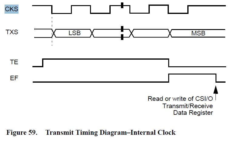
According to the Z180 datasheet, the CSIO clock (CKS) rests high, transmit is latched on a falling clock edge, and receive is latched on a rising edge. This is essentially the same as SPI mode 3 and can not be changed via control registers.
I would like to use this to control a SPI bus with a MicroSD and a 25LC rom that both operate on mode 0. I have seen a number of Z180 based SBCs [Mark IV], [SC131] that use this line to drive an SD Card.
Can somebody explain how this works? How can different spi modes operate on the same bus or is the resting state just not something most devices would care about in this type of scenario? Or is this a case of a software trick picking up the slack like mirroring the bits to be MSB first?
Thanks

Steve Cousins
Feb 9, 2022, 12:23:53 PM2/9/22
to retro-comp
I don't have answers to all of the questions in your post, but I can confirm that some Z180 software performs mirroring as you suggest. You will also find that some MicroSD adapters don't have tri-state or open collector drive on the MISO line thus don't play nice with other devices trying to share the SPI 'bus'. The MicroSD adapter used in SCxxx kits is one such device that doesn't play nice with others. It is possible to modify these particular modules if you are comfortable with cutting and soldering surface mount circuits. Another fix is to add your own tri-state buffer on the MISO line. Somewhere back in the history of this group I think there is a discussion about this.
Steve

Alan Cox
Feb 9, 2022, 1:35:07 PM2/9/22
to Steve Cousins, retro-comp
On Wed, 9 Feb 2022 at 17:23, Steve Cousins <steve...@gmail.com> wrote:
I don't have answers to all of the questions in your post, but I can confirm that some Z180 software performs mirroring as you suggest. You will also find that some MicroSD adapters don't have tri-state or open collector drive on the MISO line thus don't play nice with other devices trying to share the SPI 'bus'. The MicroSD adapter used in SCxxx kits is one such device that doesn't play nice with others. It is possible to modify these particular modules if you are comfortable with cutting and soldering surface mount circuits. Another fix is to add your own tri-state buffer on the MISO line. Somewhere back in the history of this group I think there is a discussion about this.
Almost all of the MicroSD adapters for 5v usage are unfriendly to sharing. I built a mod board for the SC126 to allow more devices and fix this - it's not actually that hard to address - you use a 1:n and n:1 mux and the problem goes away. If you are running at 3v3 it's a lot easier, just take one of that giant pile of pointless SD to MicroSD adapters you've got in the junk drawer and solder directly to the adapter to use it as the MicroSD socket.
Generally speaking the well behaved SPI devices don't care what the bus is doing when their CS line is high. Less well behaved ones have to be dealt with.
I've not tried getting a Z180 board to talk SPI 0 via CSIO. I imagine with a bit of extra logic and glue it ought to be possible.
Alan

Alastair Patrick
Feb 9, 2022, 7:46:44 PM2/9/22
to retro-comp
My understanding is, SPI modes 0 and 3 do the same things on clock edges: master and slave both shift on the falling edge and sample on the rising edge. Where they differ is the idle clock state (i.e. the state of the clock when there is no SPI bus activity.) SPI mode 3 idles the clock high but SPI mode 0 idles it low. That means an SPI mode 0 slave connected to an SPI mode 3 master will see an extraneous falling clock edge at the beginning of a packet and an extraneous rising clock edge at the end of a packet.
My guesses as to why this works are A) software is timing the lowering and raising of the chip select line such that it looks to the slave as though the clock is low when idle, i.e. SPI mode 0 and/or B) that (some?) SDCARDs are robust enough to ignore invalid clock transitions.
I have a related question. I also want to put multiple devices on an SPI bus, one being an SDCARD. My design is 3.3V throughout (built around 3.3V 8051 variant MCU.) Aside from a concern that some SDCARDs might not tristate their MISO line, I was also concerned that some might not respect their chip select and execute commands intended for other SPI devices on the bus. Has anyone seen anything like that or am I just being paranoid!?
Al
Aidan Jennings
Feb 9, 2022, 8:33:07 PM2/9/22
to retro-comp
I suppose I should have given some more practical details about what I plan on doing.

My current design is to use buffers to both the SD card and the serial EEPROM. For the SD card so the signals can be stepped down to 3.3V and for the EEPROM so I can include an ISP header to program it remotely via arduino (this idea is still a work in progress). This way the MISO lines of both devices will be passed through a buffer which will be weakly pulled high before reaching whatever device I use as the parent.
The situation that Al describes is what I am afraid of happening, but I also see some boards that seem to use the CSIO as a SPI without any additional hardware, hence my question
I know admittedly very little about the inner workings of SD cards but I have never heard of a child on a SPI bus not respecting its chip select. The only exception I can think of is this:

Mark T
Feb 9, 2022, 10:09:36 PM2/9/22
to retro-comp
The issue is not the sd card failing to respect the cs signal. The issue is with the sd card breakout boards that include a level shifter and the output of that level shifter is not tristated by the cs signal.

Alastair Patrick
Feb 15, 2022, 4:44:52 PM2/15/22
to retro-comp
I found this comment in the source code for the RomWBW SDCARD driver. TL;DR, CSIO on Z180 only talks SPI Mode 4.
; NOTES:
; 1) SIGNAL NAMES ARE FROM THE SD CARD SPEC AND ARE NAMED FROM THE
; PERSPECTIVE OF THE SD CARD (SLAVE):
; DI = DATA IN: HOST -> CARD = MOSI (MASTER OUT/SLAVE IN)
; DO = DATA OUT: HOST <- CARD = MISO (MASTER IN/SLAVE OUT)
;
; 2) THE QUIESCENT STATE OF THE OUTPUT SIGNALS (HOST -> CARD) IS:
; CS = HI (NOT SELECTED)
; CLK = LO (HI FOR CSIO)
; DI = HI (ACTIVE IS THE NATURAL/DEFAULT STATE FOR DATA IN)
;
; 3) SPI MODE 0 IMPLEMENTATION IS USED (CPOL=0, CPHA=0)
; THE DATA MUST BE AVAILABLE BEFORE THE FIRST CLOCK SIGNAL RISING.
; THE CLOCK IDLE STATE IS ZERO. THE DATA ON MISO AND MOSI LINES
; MUST BE STABLE WHILE THE CLOCK IS HIGH AND CAN BE CHANGED WHEN
; THE CLOCK IS LOW. THE DATA IS CAPTURED ON THE CLOCK'S LOW-TO-HIGH
; TRANSITION AND PROPAGATED ON HIGH-TO-LOW CLOCK TRANSITION.
;
; NOTE: THE CSIO IMPLEMENTATION (INCLUDE MK4) USES SPI MODE 4
; (CPOL=1, CPHA=1) BECAUSE THAT IS THE WAY THAT THE Z180 CSIO
; INTERFACE WORKS. ALL OF THE CLOCK TRANSITIONS LISTED ABOVE
; ARE REVERSED FOR CSIO.

7alken
Oct 7, 2023, 8:17:08 AM10/7/23
to retro-comp
ufff, cold swear ... SPI MODE 3, that "MODE 4" in code is numbering shift typo ...

Wayne Warthen
Oct 7, 2023, 10:09:54 AM10/7/23
to retro-comp
Yes, that looks like a typo on my part. Pretty sure it was supposed to be mode 3. Sorry. I will fix the comment.
-Wayne
Reply all
Reply to author
Forward
0 new messages