Help designing prototyping breakout board
360 views
Skip to first unread message

Alastair Patrick
Mar 30, 2022, 11:45:33 PM3/30/22
to retro-comp
Hi,
As part of my ongoing Z80 graphics board project, I've designed a board to help interface a 3.3V circuit assembled on a breadboard to a Z80 computer. The reason is because the RP2040 microcontroller I want to use is 3.3V and I find the level shifting logic gets out of hand on breadboards. This board could also be used to interface with CPLDs, FPGAs or other 3.3V microcontrollers.
I borrowed the address decoding logic from the SC115 breakout board and added a 74AHC245 bus transceiver to level shift the data bus and a 74AHC125 buffer to level shift A0, A1 and some control signals. The idea behind using the 74AHC series is its inputs are 5V tolerant even when powered at 3.3V.
Explanation of the headers:
There are series resistors for the data bus. These are intended to protect the bus master and the peripheral data bus if there is a bug in the Z80 interface logic where the bus master and peripheral output on the data bus at the same time. The resistors would limit current, hopefully preventing damage. These resistors can be shorted out with jumpers to bypass protection.
There are likely to be basic errors given my limited experience. I did a couple of years of electrical engineering in college before switching to software engineering but that mostly only covered analog electronics. This is the first digital circuit I've designed. I don't have any specific questions but I hoping for helpful feedback.
PDFs of schematic and PCB layout attached.
Thanks,
Al
As part of my ongoing Z80 graphics board project, I've designed a board to help interface a 3.3V circuit assembled on a breadboard to a Z80 computer. The reason is because the RP2040 microcontroller I want to use is 3.3V and I find the level shifting logic gets out of hand on breadboards. This board could also be used to interface with CPLDs, FPGAs or other 3.3V microcontrollers.
I borrowed the address decoding logic from the SC115 breakout board and added a 74AHC245 bus transceiver to level shift the data bus and a 74AHC125 buffer to level shift A0, A1 and some control signals. The idea behind using the 74AHC series is its inputs are 5V tolerant even when powered at 3.3V.
Explanation of the headers:
- PL2: D0-7 level shifted from TTL to 3.3V CMOS when for write IO requests and from 3.3V CMOS to TTL for read requests
- PL3: /RD, /WR, A0, A1, /RESET level shifted from TTL to 3.3V CMOS
- PL4: 3.3V in, /WAIT, _INT level shifted from 3.3V CMOS to TTL
- PL5: 5V out, GND
- J9: select 2 or 4 bytes of IO ports
There are series resistors for the data bus. These are intended to protect the bus master and the peripheral data bus if there is a bug in the Z80 interface logic where the bus master and peripheral output on the data bus at the same time. The resistors would limit current, hopefully preventing damage. These resistors can be shorted out with jumpers to bypass protection.
There are likely to be basic errors given my limited experience. I did a couple of years of electrical engineering in college before switching to software engineering but that mostly only covered analog electronics. This is the first digital circuit I've designed. I don't have any specific questions but I hoping for helpful feedback.
PDFs of schematic and PCB layout attached.
Thanks,
Al

Dylan Hall
Mar 31, 2022, 4:13:30 AM3/31/22
to Alastair Patrick, retro-comp
That's a cool idea, I wish I'd thought of that a year ago! I've been soldering a Pico to each prototype pcb and discovering my mistakes the hard way.

Some thoughts from my tinkering with a Pico + RC2014.
I've also settled on the AHC245 as buffers to do level conversion. I tried the LVC245. They also work and have the benefit of being faster but they are more aggressive which creates more bouncing. Early in my experiments I convinced myself this was causing issues with the Pico seeing false events, although I'm no longer convinced that was the case.
If you're willing to deal with surface mount parts, the SN74CBTD3861 and SN74CB3T3245 are both interesting. They're FET bus switches with level shifting. The first is 10 bits wide (handy if you want a couple extra bits). The second is pin compatible with regular '245 parts. They're both bi-directional so no need for a direction pin.
I'm fuzzy on using interrupts, but you may need to deal with the interrupt acknowledge event which would require some extra logic. Depending on which system you're using you may find the serial controller is already using the interrupt line which will complicate matters further.
A second row of pins for each connection may be useful. One row for connecting to the breadboard, and a second row for connecting to a logic analyser or scope.
I found while writing PIO routines to deal with I/O requests it was easier to write one routine to deal with both read and write, e.g.
wait 0 gpio, IORQ
jmp pin do_OUT ; jump based on the RD pin
do_IN: ; z80 IN, Pico write
# do something useful
jmp done
do_OUT: ; z80 OUT, Pico read
# do something useful
done:
wait 1 gpio, IORQ ; wait for the IO request to finish so we don't deal with it twice
This was useful because I could use the same FIFO for both reading and writing. If you wanted to do something similar you could connect the output of the '688 though the spare AHC32 gate as IORQ.
It's worth noting the WAIT pin is typically pulled up with a 10k resistor (I think). This means when you release it, it takes a while to rise back above 2V and for the z80 to continue executing. If I remember correctly, it's something like 10 clock cycles. If you can, it's best to use WAIT as little as possible to avoid the performance penalty or build a slightly dodgy circuit that will pull WAIT back to a high state when you're done with it.
I use the following which seems to work for me, but it may be dodgier than I realise :)
Dylan
--
You received this message because you are subscribed to the Google Groups "retro-comp" group.
To unsubscribe from this group and stop receiving emails from it, send an email to retro-comp+...@googlegroups.com.
To view this discussion on the web visit https://groups.google.com/d/msgid/retro-comp/91fc0dd9-a18d-4276-926b-a53fad38c564n%40googlegroups.com.
Alastair Patrick
Mar 31, 2022, 2:29:03 PM3/31/22
to retro-comp
Hi,
I've also settled on the AHC245 as buffers to do level conversion. I tried the LVC245. They also work and have the benefit of being faster but they are more aggressive which creates more bouncing. Early in my experiments I convinced myself this was causing issues with the Pico seeing false events, although I'm no longer convinced that was the case.If you're willing to deal with surface mount parts, the SN74CBTD3861 and SN74CB3T3245 are both interesting. They're FET bus switches with level shifting. The first is 10 bits wide (handy if you want a couple extra bits). The second is pin compatible with regular '245 parts. They're both bi-directional so no need for a direction pin.
I considered using 74CB3T3245 but decided 74ACT245, though slightly less convenient, was better because having the direction pin protects the bus master. Even if a buggy external circuit outputs to the data bus at the wrong time, hopefully only the '245 takes damage. The wrongly timed data bus output should not propagate to the bus master unless the '245 DIR pin is low, which should only happen during an appropriately addressed read IO request.
I'm fuzzy on using interrupts, but you may need to deal with the interrupt acknowledge event which would require some extra logic.
I don't intend to support interrupt mode 2, which is the Z80 interrupt mode with the complicated interrupt acknowledgement protocol. I think mostly only systems that exclusively use Z80 family peripherals use interrupt mode 2. Interrupt modes 0 and 1 are more typical from an electrical point of view; the peripheral just needs to drive /INT low until the ISR acknowledges the interrupt by reading or writing some IO port. Actually, I don't intend for my graphics board to use interrupts at all. That header pin just offers the flexibility to change my mind.
Depending on which system you're using you may find the serial controller is already using the interrupt line which will complicate matters further.
The /INT line is usually wired-OR, meaning it can be shared by several peripherals. Any peripheral can drive /INT low to raise an interrupt and, when no peripherals are doing so, /INT is pulled high by a pull-up resistor.
A second row of pins for each connection may be useful. One row for connecting to the breadboard, and a second row for connecting to a logic analyser or scope.
Good idea; I've added that.
I found while writing PIO routines to deal with I/O requests it was easier to write one routine to deal with both read and write, e.g.wait 0 gpio, IORQjmp pin do_OUT ; jump based on the RD pindo_IN: ; z80 IN, Pico write# do something usefuljmp donedo_OUT: ; z80 OUT, Pico read# do something usefuldone:wait 1 gpio, IORQ ; wait for the IO request to finish so we don't deal with it twiceThis was useful because I could use the same FIFO for both reading and writing. If you wanted to do something similar you could connect the output of the '688 though the spare AHC32 gate as IORQ.
This was actually my original plan. Since there was a leftover OR gate, I've added a /CS pin to the new revision so I can change my mind.
My plan at the moment it to have 4 Z80 IO ports: 2 for the graphics peripheral (VDP) and 2 for an emulated AY-3-8910 sound generator. The latter would output audio and, via its integrated parallel IO ports, connect to a USB keyboard and emulated MSX keyboard matrix. I intend to have 4 distinct PIO routines running to interface with the Z80 bus (i.e. one whole PIO bank) to read & write the VDP & AY-3-8910 ports. The reason is because my designs with fewer PIOs did not have sufficient flexibility to avoid unnecessary /WAIT states.
It's worth noting the WAIT pin is typically pulled up with a 10k resistor (I think). This means when you release it, it takes a while to rise back above 2V and for the z80 to continue executing. If I remember correctly, it's something like 10 clock cycles. If you can, it's best to use WAIT as little as possible to avoid the performance penalty or build a slightly dodgy circuit that will pull WAIT back to a high state when you're done with it.I use the following which seems to work for me, but it may be dodgier than I realise :)
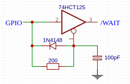
I see how that circuit works and why it speeds up deasserting the /WAIT line. /WAIT is usually wired-OR, which means a pull-up resistor is responsible for pulling it high when no peripherals are asserting /WAIT. Because of stray capacitance from the board, the rising edge could be slow. This circuit briefly drives /WAIT high, as though it were push-pull. I guess you say it's a hack because it opens the possibility of one peripheral trying to drive /WAIT high while another tries to drive it low. The selection of the resistor and capacitor values is also clock frequency dependent.
My solution to the problem is to make my VDP software "API" asynchronous so the VDP ports don't have reason to assert /WAIT at all. Only the AY-3-8910 ports will assert /WAIT. Because AY-3-8910 port accesses should be relatively infrequent compared to VDP, a slow /WAIT rising edge shouldn't be a big performance issue so I hope I won't need a similar hack.
I'm surprised it takes 10 clock cycles though. Do you mean Z80 clock cycles or RP2040 system clock cycles or other? What clock frequency?
I attached a new revision of the board design.
Al
Dylan Hall
Mar 31, 2022, 9:05:50 PM3/31/22
to Alastair Patrick, retro-comp
On Fri, 1 Apr 2022 at 07:29, Alastair Patrick <alastai...@gmail.com> wrote:
Hi,I've also settled on the AHC245 as buffers to do level conversion. I tried the LVC245. They also work and have the benefit of being faster but they are more aggressive which creates more bouncing. Early in my experiments I convinced myself this was causing issues with the Pico seeing false events, although I'm no longer convinced that was the case.If you're willing to deal with surface mount parts, the SN74CBTD3861 and SN74CB3T3245 are both interesting. They're FET bus switches with level shifting. The first is 10 bits wide (handy if you want a couple extra bits). The second is pin compatible with regular '245 parts. They're both bi-directional so no need for a direction pin.I considered using 74CB3T3245 but decided 74ACT245, though slightly less convenient, was better because having the direction pin protects the bus master. Even if a buggy external circuit outputs to the data bus at the wrong time, hopefully only the '245 takes damage. The wrongly timed data bus output should not propagate to the bus master unless the '245 DIR pin is low, which should only happen during an appropriately addressed read IO request.
That's a good idea, I made a number of mistakes in my PIO code that resulted in the Pico trying to drive the data bus at the same time as another device.
I see how that circuit works and why it speeds up deasserting the /WAIT line. /WAIT is usually wired-OR, which means a pull-up resistor is responsible for pulling it high when no peripherals are asserting /WAIT. Because of stray capacitance from the board, the rising edge could be slow. This circuit briefly drives /WAIT high, as though it were push-pull. I guess you say it's a hack because it opens the possibility of one peripheral trying to drive /WAIT high while another tries to drive it low. The selection of the resistor and capacitor values is also clock frequency dependent.
I don't think the clock frequency matters, the enable line on the '125 lags behind the output by about 20ns which is long enough for the gate to pull WAIT above 2V. And I agree, the risk is two devices competing for the WAIT line at the same time. My hope is that given the short period of time where it pulls the line up that no damage is likely to occur.
I'm surprised it takes 10 clock cycles though. Do you mean Z80 clock cycles or RP2040 system clock cycles or other? What clock frequency?
Sorry, I've confused myself here. I was initially tinkering with a Z180 @ 18Mhz and I have a rubbish memory :) I think the delay is about 250-500ns. In other words, it's probably not a big deal, ignore me!
The following is while I was testing different ways of driving the WAIT line (in this case with a 2N2222). Blue is WAIT and red is the GPIO output.

Dylan
Alastair Patrick
Apr 2, 2022, 2:32:06 PM4/2/22
to retro-comp
I think the "dodgy" circuit to briefly drive /WAIT high is safe in the context it's used and I've incorporated it into my new revision (attached) in a way that I can leave it unpopulated if I don't want it. I verified this because I was considering adding it to my design, not because I thought it didn't work btw :) Here's my reasoning as to why it's okay.
t = -200*100e-12*ln(1-2/5)
=~ 10ns
While a peripheral is servicing an IO request, the earliest any other part of the circuit ought to drive /WAIT is the falling clock edge of the next T1 cycle. So it should be safe for the peripheral to drive /WAIT, either low or high, until the falling clock edge of the next T1 cycle. In the worst case, the peripheral will begin to drive /WAIT high just before the falling clock edge of the IO request's T3 cycle. Note that If it begins to drive it high just after the falling clock edge, it's actually a wait state (TW) cycle rather than a T3 cycle and the T3 cycle will be the next cycle.
The time between the falling clock edge of the T3 cycle and the falling clock edge of the following T1 cycle is one clock cycle. For a 20MHz clock, that's 50ns. That's all I meant when I said I thought the circuit was clock rate dependent.
The formula for the voltage across a capacitor in an RC delay circuit is:
Vc = Vs*(1-exp(-t/R*C))
or equivalently:
t = -R*C*ln(1-Vc/Vs)
For the components in the circuit posted:
t = -200*100e-12*ln(1-2/5)
=~ 10ns
< 50ns
Perhaps a more satisfying (less dodgy?) circuit to implement this would be one that ceased driving /WAIT high on any rising clock edge while /IORQ was high, i.e. on the boundary between T3 and T1 cycles. I can't think how to do that without using more components though.
I also incorporated a protoboard area. A question relating to that. I know protoboard is available both with and without solder mask. I've never used protoboard but it seems that not having solder mask might be beneficial for dragging solder between pads. Does anyone have an opinion as to whether protoboard with or without solder mask is better and why? Obviously if I removed the solder mask from that area, I would exclude the copper pour too.
Thanks,
Al

Mark T
Apr 2, 2022, 6:57:04 PM4/2/22
to retro-comp
It can be tricky using wait on a 20MHz z80. If you use MREQ or RD these are up to 40ns after falling edge of T1 but the set up time for wait is 7.5 ns before the falling edge of T2. This gives you 2.5ns for propogation delay of the circuit to activate wait. Typical timing of z80 might give a bit more time but might be temperature and voltage dependent.
One way round this is to consider /WAIT as DTACK, hold it low and release it when the memory device is ready. But that could be a problem with your active pullup at the end of a wait cycle.
Another possibility is to use IORQ high to indicate a memory cycle as this gives you a bit more time to activate wait.
Trying to wait only on write cycles is even worse as /WR is only active after T2. It can be done using MREQ active or IORQ inactive and RD inactive.
Alastair Patrick
Apr 2, 2022, 8:30:26 PM4/2/22
to retro-comp
Hi Mark,
For this project, I'm only concerned about asserting /WAIT in response to read IO requests, which have a bit more slack than M1 memory reads with regards to timing, which is what I think you're basing 2.5ns on.
I hope it'll be possible for the RP2040 microcontroller to assert /WAIT quickly enough for a 10MHz Z80 or a 20MHz Z180 but not a 20MHz Z80. The Z180 can be software configured with additional memory and/or IO automatic wait states. As configured by RomWBW, which is what I'm primarily concerned with, Z180 systems generate one additional IO automatic wait state, i.e. two wait states total. Z180 timing is also easier for read IO requests because /IORQ and /RD fall relative to the falling edge of T1 rather than the rising edge of T2 as on Z80.
Based on that, this is how much time the RP2040 microcontroller has to detect its /RD or /WR pin going low and assert /WAIT.
Z80 @10MHz
150ns T2 rising edge to TWA falling edge
-50ns /IORQ or /RD delay after T2 rising edge
-9ns 74HCT688 E to output propagation delay
-5ns 74AC32 high to low propagation delay
-4ns 74AC125 propagation delay
-20ns /WAIT setup time
----
62ns remaining
Z80 @20MHz
75ns T2 rising edge to TWA falling edge
-40ns /IORQ or /RD delay after T2 rising edge
-9ns 74HCT688 E to output propagation delay
-5ns 74AC32 high to low propagation delay
-4ns 74AC125 propagation delay
-7.5ns /WAIT setup time
----
9.5ns remaining
Z180 @20MHz configured with one additional automatic IO wait state
150ns T1 falling edge to second TWA falling edge
-25ns /IORQ, /RD delay after T2 rising edge
-9ns 74HCT688 E to output propagation delay
-5ns 74AC32 high to low propagation delay
-4ns 74AC125 propagation delay
-15ns /WAIT setup time
----
92ns remaining
The RP2040 PIO processors have one cycle instruction latency and have an instruction to wait for a pin to go low. So that's potentially 2 instruction cycles to bring /WAIT low. RP2040 also has a 2 cycle input synchronizer to mitigate hazards and meta-instabiity, which can be turned on or off per pin. One RP2040 cycle is about 8ns so it should take 16-32ns for the RP2040 to assert /WAIT depending on whether the pin synchronize is active.
Al
Alastair Patrick
Apr 8, 2022, 4:47:37 PM4/8/22
to retro-comp
Dylan,
I realize now that interfacing 3.3V logic with the Z80 data bus using a 74AHC245 bus transceiver is actually not robust. One of the reasons 74AHC series inputs are 5V tolerant at 3.3V supply is because, unlike other CMOS logic such as 74HC series, 74AHC series inputs lack ESD protection diodes to VCC. Connecting the input in the schematic below to 5V causes no problem, even if VCC is 3.3V.
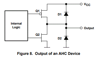
Unfortunately, that is not true of 74AHC outputs, which do have ESD protection diodes to VCC. The danger is, connecting 4-5V to the output in the schematic below, even if the output is tri-stated, current would flow through D1 and backward into VCC.
I think one of the A 5V tolerant FET bus switches mentioned should work without issue.
Al
Mark T
Apr 8, 2022, 5:11:57 PM4/8/22
to retro-comp
That is an interesting point.
I took a look at the nexperia data sheet and it does only say that inputs are 5v tolerant, but also says these buffers can be used for level shifting, though they do have outputs on each side of the buffer.
The TI data sheet for 74lvc245 also says inputs are 5v tolerant., but also says 5v input/output voltages on all ports. It also shows an example of the 74lvc245 as a level shifter.
Alastair Patrick
Apr 8, 2022, 6:18:38 PM4/8/22
to retro-comp
Great! Yes 74LVC245A should work. Below is an excerpt from the LVC Designer's Guide. Emphasis mine.
"Since the LVC family uses a 3.3-V power supply, interfacing LVC devices with other components that use a 5-V power
supply becomes a concern. If a low-voltage device is subjected to a 5-V presence at its inputs or outputs, it is critical
that the device is not damaged. The term 5-V tolerance is used to imply that a presence of 5-V at either the input or
output of a device will not damage it. Whether a device is capable of tolerating a 5-V presence only at the input, only
at the output, or at both the input and output must be considered. As a result, when determining whether a device
is considered to be 5-V tolerant, several issues must be addressed.
Every LVC device TI produces can be subjected to a 5-V presence at its input and not be damaged. This includes
all of the gate-function, octal, and Widebus devices. Thus, all of TI’s LVC devices are 5-V input tolerant.
Whether or not an LVC device can be subjected to a 5-V presence at its output requires further consideration. For
the term 5-V output tolerant to be meaningful, the outputs of the device must be capable of being placed in the
high-impedance state. Two LVC gate functions, all LVC octals, and all LVC Widebus devices have 3-state outputs,
and it is to these devices only that the term 5-V tolerance applies. (The LVC gate functions that do not have 3-state
outputs should not be connected to a bus and, therefore, should not be subjected to a 5-V presence. This means that
5-V output tolerance does not make sense for these devices since their outputs cannot be placed in the
high-impedance state.) For those devices with outputs capable of being placed in the high-impedance state, 5-V
output tolerance means that a presence of 5 V at its output does not damage the device.
TI is naming all 5-V tolerant devices with an A after the device number. For example, LVC16245A indicates that the
device is 5-V tolerant. All LVC devices are 5-V input tolerant, and an A in a device name indicates that, if appropriate,
the device is also 5-V output tolerant."
Al
Mark T
Apr 8, 2022, 8:04:28 PM4/8/22
to retro-comp
I think I would still expect it to be safe to connect the output of a 74lvc with 3.3v Vcc to the input of a 74(A)(H)CT with 5v Vcc due to the high input impedance. Probably not a good idea with 74(A)(L)(S)(F) though.
The other thing I noticed recently is that although the 74LVC devices are not recommended on 5v Vcc the single gate 74LVC1g range do include 5v Vcc as an option. They also have Ioff circuit to protect the output when they are turned off.
Dylan Hall
Apr 9, 2022, 6:19:30 AM4/9/22
to retro-comp
Hi, I'm a little out of my depth here. Do I have the following right?
Assuming the bus signals are at 5V, the AHC parts are at 3.3V, and for arguments sake D1 conducts at 0.7V then the bus signals will be pulled down to 4V and the 3.3V power supply will be sinking the difference via the AHC part.
If that's the case, what about this causes an issue?
Does this risk damaging D1 because it's carrying too much current? (no resistor to limit it)
Does this risk damaging whichever part is driving the 5V signal by pulling too much current?
Is it poor form to mess with the levels on the bus?
I have a couple test boards, one with AHC245 parts and I think another with LVC245 parts. I'll try connecting with them one at a time and see what impact they're having.
Thanks,
Dylan
--
You received this message because you are subscribed to the Google Groups "retro-comp" group.
To unsubscribe from this group and stop receiving emails from it, send an email to retro-comp+...@googlegroups.com.
To view this discussion on the web visit https://groups.google.com/d/msgid/retro-comp/93a81075-5043-43ef-9796-b0bb361bc210n%40googlegroups.com.
Alastair Patrick
Apr 9, 2022, 10:32:05 AM4/9/22
to retro-comp
I'm a beginner but this is what I think might happen in various scenarios, some more realistic than others. In all cases, 74AHC245 is connected directly to a Z80 data bus.
1) The data bus line is pulled high by 10K resistors. With nothing else connected, the data bus will be 3.3V + D1 drop = 4V. 100uA flow through the resistors and D1. Nothing bad happens.
2) A data bus line is driven high by 74LS series logic with a typical TTL VOH (high output voltage) of 3.4V. Nothing bad happens because 3.4V does not overcome D1's forward voltage.
3) Same as above but with 74HCT logic. If the 3.3V power supply is capable of regulating while sinking current, VOH is 3.3V + D1 drop = 4V. The current flowing through D1 is whatever is needed to make 74HCT logic VOH fall to 4V, probably a few mA. Maybe that will damage D1? I don't know enough about AHC. 74HCT can safely source a few mA. There's maybe some potential for damage here for components can't source sufficient current. Probably nothing bad happens.
4) The assumption that the 3.3V power supply can regulate while sinking current in 3) isn't necessarily realistic. Suppose the 3.3V circuit only draws a few uA, not enough to make VOH fall much below 5V. What could actually happen is, because the 3.3V power supply is no longer able to regulate while sinking current, VCC for the 3.3V circuit rises to 5V - D1 drop = 4.3V. 4.3V is outside the absolute maximum VCC for many 3.3V components.
Al
Mark T
Apr 9, 2022, 11:39:40 AM4/9/22
to retro-comp
Another risk is latch up, but I think its unlikely that anything on the data bus would be able to drive more than 100mA into one of the output pins.
I didn’t register to see the spec referenced by the 74ahc245 data sheet but this stack exchange link gives some indication of the latch up spec.
I think I’d be more concerned about any loading of the rom or ram data outputs.
Reply all
Reply to author
Forward
0 new messages