Improving ground and power on proto boards
110 views
Skip to first unread message

Mark T
Nov 6, 2022, 5:36:37 PM11/6/22
to retro-comp
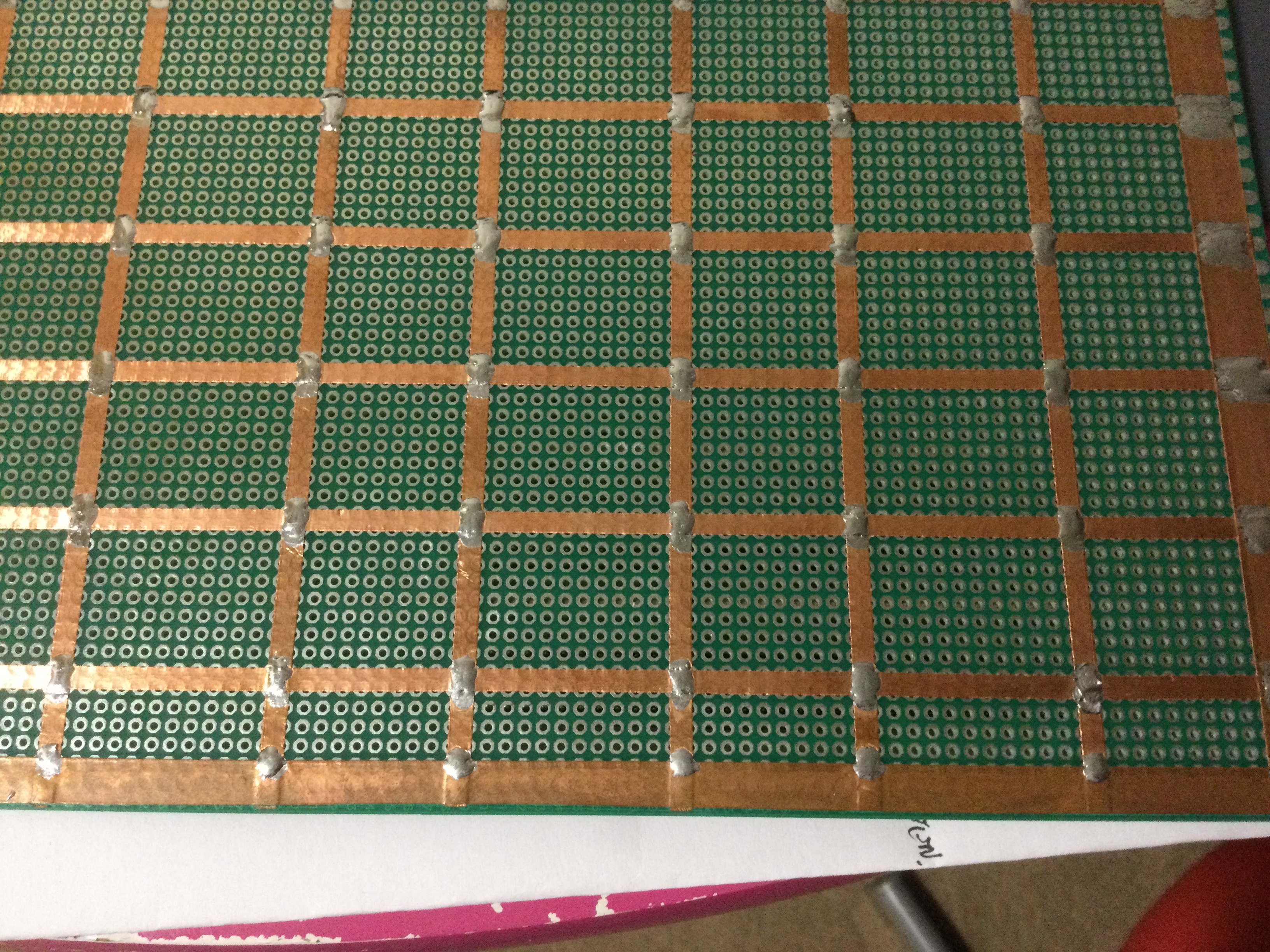
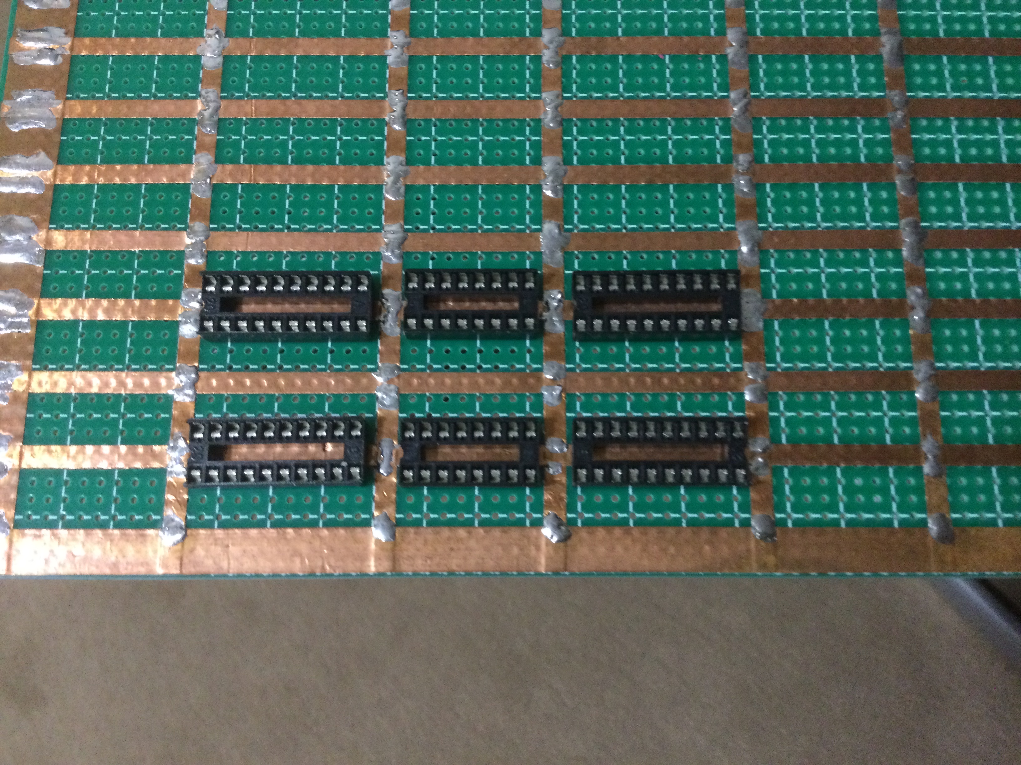 This is just an idea to improve ground and power on proto boards where most of the wiring will be point to point. I guess it could also be used with wire wrap. Starting with single sided prototype board with one pad per hole, then run a grid of copper tape on the top side of the board for ground plane and then a second grid of copper tape on the pad side for 5v. I chose top side for ground as I use top side for longer runs of wiring and bottom side for short runs between adjacent ICs. I’ve used 3.2 mm wide copper tape as this seems to fit well under ICs and between pads. The photos attached as example alternate between 20 pin and 16 pin IC sockets as I’ll be using a mix of IC sizes. Although the adhesive is supposed to be conductive the grid should be soldered at each crossing.
Douglas Miller
Nov 8, 2022, 10:41:35 PM11/8/22
to retro-comp
With the ease of making custom PCBs these days, seems like one could just layout a PCB for prototyping and go with that.
Back in the day, I used a very handy pattern for wire-wrap, but it could probably be modified for point-to-point. I have some scraps of that board:
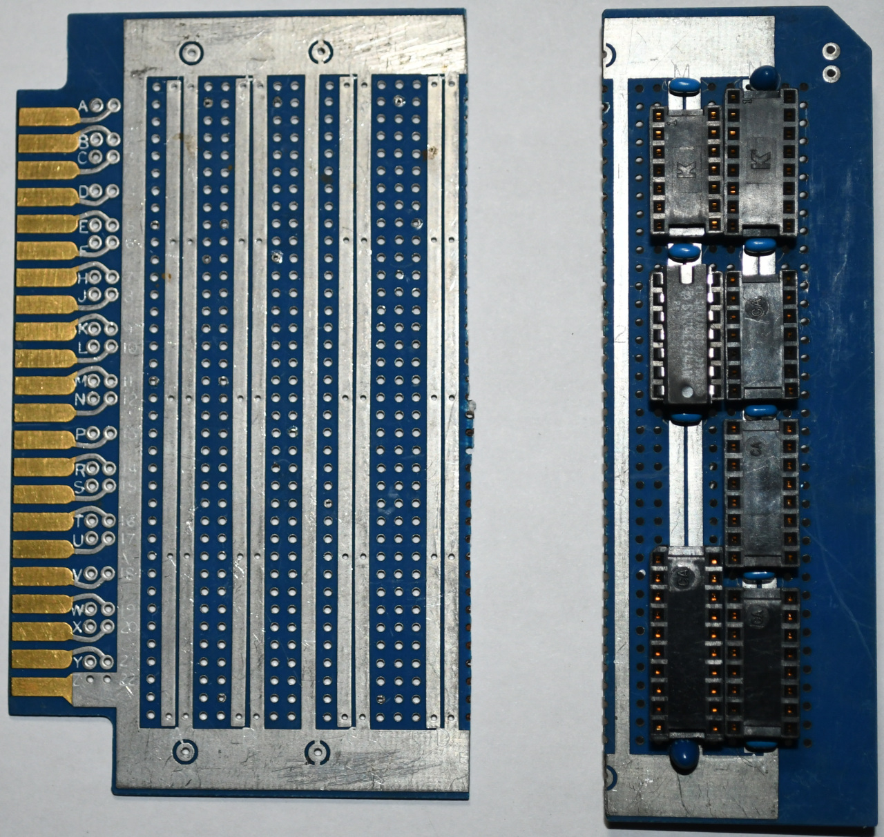
I did a kicad layout using this pattern (rendered with solder mask but that would be removed):
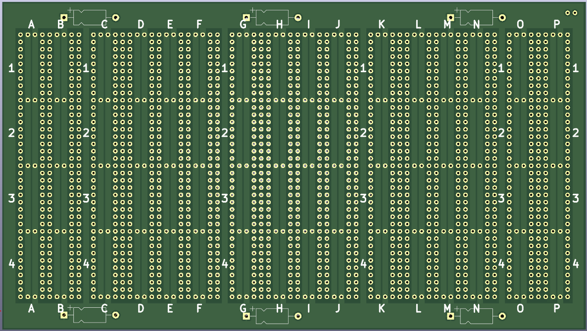
The pattern has strong power and ground, and space for lots of bypass and filter caps. It can handle 0.3 or 0.6 DIPs easily. Just an example of what could be done.
Mark T
Nov 9, 2022, 1:45:46 AM11/9/22
to retro-comp
I need a larger area than I thought would be cost effective from JLCPCB. I think 200 x 300 mm would be enough if I designed a proto pcb layout but I don’t think I’ll be doing anything like this more than once so a set of five boards would probably be wasted.
If I did make a proto board I would probably put ground fill on the top side with pad size small enough to fill ground between holes. Then power grid would still be on the bottom side. It might be possible to avoid the excess drilling fee charged by JLCPCB if the strips under the rows of DIL sockets are not drilled but its going to be a close call. I guess they have had a lot of people ordering proto boards from them lately.
This is for a first attempt at a 16 bit pipelined processor with a mix of 74F, 74AS and 74ACT, and I’m expecting a lot of redesigns and rewiring on the way. If I had more confidence it might have been worth going straight to pcb, possibly in byte slice pcbs.
Douglas Miller
Nov 10, 2022, 9:53:30 AM11/10/22
to retro-comp
My point was that a well thought-out pattern would be applicable to a larger audience (result in larger volumes). One of the ideas inherent in the pattern I showed is that improved power/ground also needs bypass and filter caps. I'm not sure how you are planning to add those into this pattern, or how you plan to connect the top foil to the corresponding pin on the DIP socket. I can't comment on the cost of these boards, and certainly the amount of drilling required for prototype boards is a factor - which is probably why most prototype boards I've bought "off-the-shelf" have pretty uneven, inconsistent, holes and nothing through-hole-plated. Every time I have to use one of those, I think about trying to recreate the boards I used to use (shown above).
If you're expecting to make changes, you might want to consider wire-wrap. But, if you're not setup for that or haven't spent time doing wire-wrap, that would be a hurdle. Tools are more expensive, and (of course) learning to use them correctly is important, but you have a much better chance of (successfully) making changes later.
Sounds like you are planning a large and complex project. It will be interesting to see the finished product.
Mark T
Nov 10, 2022, 11:07:52 AM11/10/22
to retro-comp
Plan for ground connection is a link of tinned copper wire from the ground pin through the board using an adjacent hole onto the nearby point where the tapes cross. Decoupling caps to be mounted close to the power pins, soldered to ground on top side where the tapes cross, then through the board to the power pin, with a short link between the capacitor vcc and the copper tape, so power goes first to the capacitor and from there to the IC.
I’ll start a thread with the datapath when I finish a few changes. I recently bought an old copy of Hennessy and Patterson, Computer Organisation & Design, which I think is slightly easier reading than Computer Architecture A Quantative Approach. Most of the information can be found on the internet but its nice to have all in one book. I’m making quite a few changes due to the 16 bit limit as it doesn’t fit well with separate registers for destination and two sources.
I keep changing my mind on implementation of the registers, but likely to be 16 registers using half of each 74AS870. Original plan was 32, but setup and hold time on the select inputs is probably going to limit me to use only one of the 16x4 sets from each chip with the select lines hard wired.
Reply all
Reply to author
Forward
0 new messages