6502 CPU & Logic Card Design for z50 bus
186 views
Skip to first unread message

Individual Solid
Mar 5, 2023, 2:18:18 AM3/5/23
to retro-comp
Hey folks,
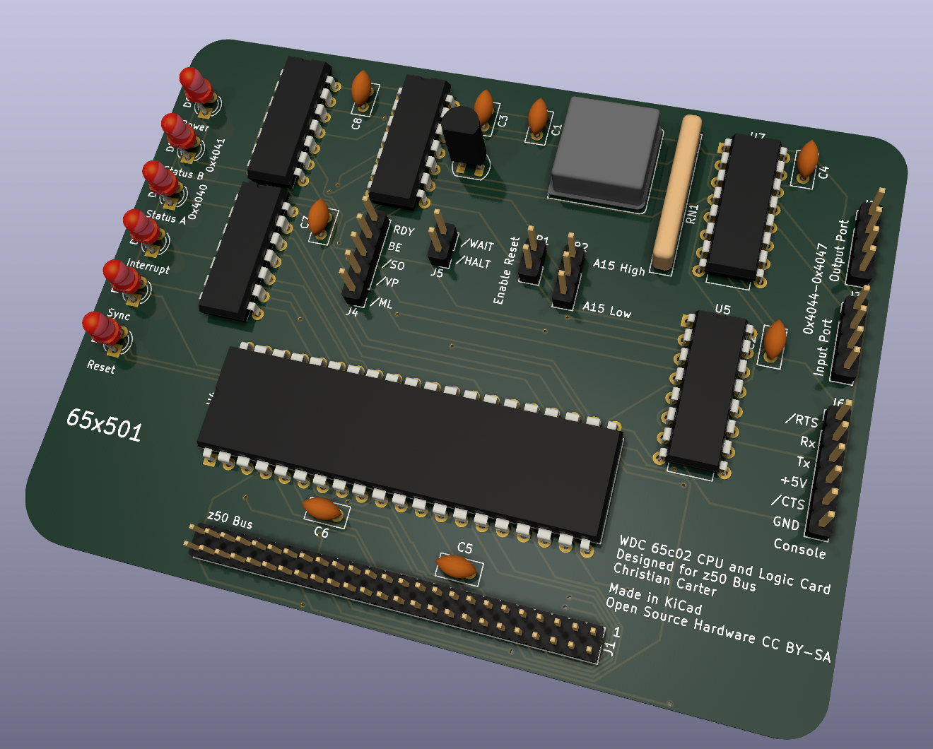
My board is designed to provide the CPU and bus logic signals, and to be compatible with the following cards:
SC502 9V-12V Power and Reset card OR
SC526 5v Power and Reset card
SC519 [url=https://smallcomputercentral.com/sc519-z80-memory-card-z50bus/]RAM/ROM card
As well as being generally compatible with other z50 bus cards that don't rely on the z80's special interrupt handling (e.g. not the z80 CTC/PIO/SIO accessories).
The board generates the following z50 bus signals.
/RD and /WR (thanks to BDD's great circuit)
/IOReq at $4000-$8000 (thanks to Garth's memory map
/MReq (simple NOT /IOReq)
/M1 (simple NOT SYNC)
In order to support the standard z50/z80 memory map and existing memory cards, there is a jumper to export either A15 or /A15 to the bus on the A15 line. By selecting the /A15 option, the existing memory card can be used, its RAM and Flash accesses will be flipped.
There's eight 1-bit inputs and eight 1-bit outputs onboard, selected by the /PORT signal. A 74HC4075 generates /PORT as well as the chip enables (/PORT & /IOReq & the appropriate read or write). These offer a bit-banged UART, two status LEDs that can be controlled by the user program, and four bits on headers for user experiments. The output circuit comes from SCC's SC519/SC516 designs, and I just tried to flip/reverse it for the input port.
BE/RDY/SO/VP/ML are all just tied high (or left floating where appropriate) but a header exposes them, in case I want to bodge on some logic later. The bus standard specifies /WAIT and /HALT signals but no existing peripherals use them, and I haven't quite figured out what splitting RDY for that would look like anyway.
I'm attaching a draft schematic (in color and B&W). I'd appreciate any comments, suggestions, or pointing out any mistakes I've made. All logic is 74HCxx series (even if I maybe forgot to update the symbol) running at 5V.
A few specific points I'd like feedback on:
1) the single bit ports all use the LSB of the data bus for actually communicating with the processor. Is there a bit that's easier to read/write consistently, that I should consider instead of D0?
2) Does this Mux actually work the way I'm trying to use it?
3) I stuck all the resistors for the LEDs under the CPU, I'm thinking a second resistor net is a better idea, but I haven't priced components yet. practically, how does the price of a thru-hole resistor net compare to that of a handful of thru-hole resistors?
4) I wanted to provide an LED for /HALT but I ran out of gates to even invert it, let alone figure out how to connect it to RDY. Is there any simplification in my logic that would bring net me a spare inverter?
Many thanks!
I just posted this over on 6502.org but I have the first draft of a schematic for a WDC65C02 card for the z50 bus, compatible with the SC519 RAM/Flash module:
Schematic attached as well...
SC502 9V-12V Power and Reset card OR
SC526 5v Power and Reset card
SC519 [url=https://smallcomputercentral.com/sc519-z80-memory-card-z50bus/]RAM/ROM card
As well as being generally compatible with other z50 bus cards that don't rely on the z80's special interrupt handling (e.g. not the z80 CTC/PIO/SIO accessories).
The board generates the following z50 bus signals.
/RD and /WR (thanks to BDD's great circuit)
/IOReq at $4000-$8000 (thanks to Garth's memory map
/MReq (simple NOT /IOReq)
/M1 (simple NOT SYNC)
In order to support the standard z50/z80 memory map and existing memory cards, there is a jumper to export either A15 or /A15 to the bus on the A15 line. By selecting the /A15 option, the existing memory card can be used, its RAM and Flash accesses will be flipped.
There's eight 1-bit inputs and eight 1-bit outputs onboard, selected by the /PORT signal. A 74HC4075 generates /PORT as well as the chip enables (/PORT & /IOReq & the appropriate read or write). These offer a bit-banged UART, two status LEDs that can be controlled by the user program, and four bits on headers for user experiments. The output circuit comes from SCC's SC519/SC516 designs, and I just tried to flip/reverse it for the input port.
BE/RDY/SO/VP/ML are all just tied high (or left floating where appropriate) but a header exposes them, in case I want to bodge on some logic later. The bus standard specifies /WAIT and /HALT signals but no existing peripherals use them, and I haven't quite figured out what splitting RDY for that would look like anyway.
I'm attaching a draft schematic (in color and B&W). I'd appreciate any comments, suggestions, or pointing out any mistakes I've made. All logic is 74HCxx series (even if I maybe forgot to update the symbol) running at 5V.
A few specific points I'd like feedback on:
1) the single bit ports all use the LSB of the data bus for actually communicating with the processor. Is there a bit that's easier to read/write consistently, that I should consider instead of D0?
2) Does this Mux actually work the way I'm trying to use it?
3) I stuck all the resistors for the LEDs under the CPU, I'm thinking a second resistor net is a better idea, but I haven't priced components yet. practically, how does the price of a thru-hole resistor net compare to that of a handful of thru-hole resistors?
4) I wanted to provide an LED for /HALT but I ran out of gates to even invert it, let alone figure out how to connect it to RDY. Is there any simplification in my logic that would bring net me a spare inverter?
Many thanks!

Jacob Krall
Mar 5, 2023, 10:32:46 AM3/5/23
to retro-comp
> Is there a bit that's easier to read/write consistently, that I should consider instead of D0?
Individual Solid
Mar 5, 2023, 1:03:27 PM3/5/23
to retro-comp
Oops, the actual schematic didn't attach!
Ah yes, I knew something about D7 was lodged in my head. Thanks!
One errata already: the decoupling caps should be 100nf, not 100uf!
> Yes, use D7 or D6 as they are easily read with the BIT opcode.
Individual Solid
Mar 5, 2023, 1:37:47 PM3/5/23
to retro-comp
Another question/point of discussion -
To support the 65c51, 65c21 and 65c22 interface adaptors, I'll need to export the actual CPU /RW signal to the bus instead of using the 8080 signals that are clock qualified. Obviously, this could be jumpered to a USR pin and jumpered back on support boards, but that seems a little tacky. I'm thinking about reusing /REFRESH since that signal is meaningless in the 6502 ecosystem and no z50 bus peripherals that I'm aware of use it anyway.

Alan Cox
Mar 5, 2023, 2:30:08 PM3/5/23
to Individual Solid, retro-comp
For inputs I would use D7. The CPU can test several of them fast but for rotating bits into something it is much easier to use 0 and 7. That will help with bitbang serial and also when your board does what all boards do and grows up to bitbang an SD card 8)
Do you know what software you plan to run, does the memory map work for that - eg if you want to run DOS65 ?
On Sun, 5 Mar 2023 at 18:03, Individual Solid <cdca...@gmail.com> wrote:
Oops, the actual schematic didn't attach!
Some of the input/output arrows look backwards which if you are using Kicad will probably make the design check tools barf.
Little one: I think your M1 is not going to work out. M1 is also used by the Z80 for interrupt acknowledge cycles and I think your M1 off the 6502 plus the other decodes will at times generate false interrupt acks. You can probably just pull it high (or maybe jumper it either way to experiment). Lots of jumpers is good when testing stuff 8).
Big one: It looks to me like it will probably work with old parts (Rockwell etc) but not the current WDC parts.
At the end of a valid bus cycle your CLK will send \WR and \RD back high. There's a propagation delay through those gates so they will rise some number of nanoseconds after the clock. At the point the clock rises your address and data bus lines go invalid. so your IORQ/MREQ will also no longer be valid about the same time as the other lines.
For read this should be fine. The CPU samples as or before it changes the clock edge so it will get valid data. It might flap about momentarily but you are probably safe unless IORQ glitches and a memory read turns into an I/O read. That might break but you'd have to draw out the timing to check what can happen.
For write however the device will see
Address lines valid
Data lines valid
IORQ valid
\WR low
..... time passes ...
Data lines invalid
\WR high
which doesn't work.
The older 6502/C02 chips like most processors have what is called a "write hold" time where they hold the data lines valid for 30-40ns after the rising clock edge. That's enough to cope with your propagation delays (just about) and work with most hardware.
The current WDC chips don't do this. It's one of the changes they made to run at higher speed. On a small SBC with parts using RW it works because there's enough stray capacitance to save your bacon. On a backplane you lose.
My 6502 card for RCBus started out roughly like yours (minus any onboard I/O and with I/O at $FExx via a 74HCT688 - which gave me even more IORDY/MREQ skew than you have). It works beautifully with Rockwell and similar parts but not with a WDC part.
The final design I ended up having to use a few gates to create a delay chain so that the CPU was fed off the delayed clock but the WR and RD lines were gated on the original clock.
I'd suggest you check the pin out differences for the older parts and stick a few jumpers on so you can try them too if you have problems with timing.
Other thing to be aware of - which you may well know - the Z80 peripheral chips used on most Z50bus cards will not easily work with anything but a Z80. They have some rather deep and magical knowledge of the CPU internals and exact clock behaviour. The 68B50 cards also tend to have problems because the hack used to interface them to a Z80 bus doesn't work so well with a non Z80 part.
Alan
Individual Solid
Mar 5, 2023, 3:02:47 PM3/5/23
to retro-comp
Alan,
Many thanks for the input! Do you have a link to the schematic for your RCBus 6502 card? I'd love to see roughly what your Mreq/IOReq circuits look like.
I have avoided drawing out the timing diagrams so far, but you're making a convincing argument that I should actually do that work. I'll admit, I slapped an 4MHz can on the board instead of an 8MHz hoping it'd allow me to skip some of these concerns. But I absolutely want this to work with modern 65c02 parts from WDC so some investigation is definitely warranted. I do not personally need this to work with older e.g. Rockwell 6502s, so I'm avoiding jumpers for the pin differences.
RE: input/output labels - you're right, I got a little lazy at the end and need to go back and update some of those net labels. Good catch.
I hadn't intended on running DOS65 or even any particular software, I have a bit of a homegrown boot loader kernel from my breadboard machine and was going to adapt that. So, the memory map doesn't really matter much. However, the map is based on Garth Wilson's 6502 Primer circuit, so a lot of 6502 code expects this RAM/ROM/IO window, and it's trivial to connect a 65c22 VIA to the same addresses Garth (and Ben Eater) use.
To be honest, I wasn't really sure if providing a decoded /M1 was necessary at all. None of the peripherals I'm planning on using require an /M1 signal (and obviously there's no Interrupt Ack on 65x family devices). Maybe I should switch that inverter to provide a halt status LED instead, but idk, I had a small inkling perhaps a front panel or bus monitor might want to snoop on the /M1 or SYNC signal.
Acknowledged read z80 family peripherals. I do not intend to use those parts, but I would like the board to be compatible with e.g. the simple digital IO module.
Alan Cox
Mar 5, 2023, 8:16:53 PM3/5/23
to retro-comp
On Sun, 5 Mar 2023 at 20:02, Individual Solid <cdca...@gmail.com> wrote:
>
> Alan,
>
> Many thanks for the input! Do you have a link to the schematic for your RCBus 6502 card?
The 65C816 card is basically the same and is here.
>
> Alan,
>
> Many thanks for the input! Do you have a link to the schematic for your RCBus 6502 card?
https://hackaday.io/project/170566-65c816-for-rc2014
This is not a particularly nice way to do it. In particular the way I
have RD handled is definitely wrong - WR needs to drop earlier than
the CPU thinks, but RD needs to drop when the CPU says so. In other
words RD should probably be coming off CLK0 but CLK but then MREQ/IORQ
might be out of order
so might need something like the IORQ/MREQ gated accordingly so MREQ
is seen for any excess read time (Isn't this fun)
It works as is (I found the \RD bug much later by inspection).
The actual board uses a 74HCT00 for the skewing as the 74AHC was too
fast. It's not really how you are supposed to do such things and
probably has real electronic engineers yelling "nooooo...."
Individual Solid
Mar 5, 2023, 9:21:30 PM3/5/23
to retro-comp
Aha, seeing the clock delay you've built made a little more sense to my brain than reading about it. Thanks! I'm going to have to sit down and think through my timings. I can shove another hex inverter on the board, there's room if I push the spare control signal headers off to the edge where they probably should be anyway. After adding a few gate delays on the clock I might just be at the point where I want to go to fab and see what the signals look like under the scope. I better make sure I add some test points for internal only signals too.
Reply all
Reply to author
Forward
0 new messages