RE: KiCAD query - through holes + SMD raspberry pi connector

Alex Gibson
PLEASE NOTE THIS IS A (slightly) FOR-PROFIT PROJECT – I would be glad to give a finished PCB to anyone who can help J
Hi all
I’m making an HX711 load cell amplifier HAT for raspberry Pi. I needed one, and wanted a relatively simple end to end project to refresh my KiCAD knowledge, which is limited.
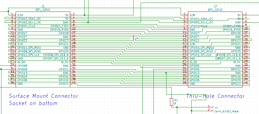
In KiCAD I am using a template for a Raspberry Pi Zero HAT which includes components and footprints for both a SMD and through-hole 40-pin connector:
https://github.com/mikelawrence/RPi_Zero_pHat_Template
I’ve used both connector footprints, overlapping, to give options – but the through-hole version is not a plated through hole with a pad on both sides – instead it’s only pads on the front side which are connected to nothing right now – everything is happening on the back side.
Is there a neat way to join these together without adding 40 separate vias? Do I have to edit the 40-pin through hole component to include pads on both sides?
Also - I am looking to get these made by PCBWay ASAP – Anyone able to review whether there’s anything sub-optimal about the design?

In the schematic I’ve already joined all the pins of one connector to all the pins of the other…

Thanks,
Alex Gibson
admg consulting
edumaker limited
· Project management
· Operations & Process improvement
· 3D Printing

Mark Robson
--
You received this message because you are subscribed to the Google Groups "rLab / Reading's Hackspace" group.
To unsubscribe from this group and stop receiving emails from it, send an email to reading-hacksp...@googlegroups.com.
For more options, visit https://groups.google.com/d/optout.

Richard Ibbotson
As Mark said, do a quick custom footprint with plated Holes. I don’t see how you can build it without plated holes and pads on the rear of the board. I understand your indecision between through hole and SMT, through hole component cost less at low volume and hand build, but assembly of SMT cheaper in volume. I would go with through hole to suit your own needs, then if some Chinese company want to copy and do volume, they can figure that out.
Not seeing you full design, but beef up the power rails and think about decoupling capacitor location and analog ground plane if you want good performance.
From: reading-...@googlegroups.com <reading-...@googlegroups.com> On Behalf Of Mark Robson
Sent: Monday, January 28, 2019 3:41 PM
To: reading-...@googlegroups.com
Subject: Re: [RDG-Hack] RE: KiCAD query - through holes + SMD raspberry pi connector
Why not use plated through-hole as a normal 40-pin header would? What's the problem?
Also, on your schematic, please use global labels for GND and +5, etc. Or named nets for everything, like they do on the actual Pi Zero schematic:
I think it would be better to create a custom footprint which includes the pads for both types of connectors (a "composite") and has plated holes. That would make the schematic simpler and be less hacky.
Mark
On Mon, 28 Jan 2019 at 12:50, Alex Gibson <al...@alexgibson.net> wrote:
PLEASE NOTE THIS IS A (slightly) FOR-PROFIT PROJECT – I would be glad to give a finished PCB to anyone who can help J
Hi all
I’m making an HX711 load cell amplifier HAT for raspberry Pi. I needed one, and wanted a relatively simple end to end project to refresh my KiCAD knowledge, which is limited.
In KiCAD I am using a template for a Raspberry Pi Zero HAT which includes components and footprints for both a SMD and through-hole 40-pin connector:
https://github.com/mikelawrence/RPi_Zero_pHat_Template
I’ve used both connector footprints, overlapping, to give options – but the through-hole version is not a plated through hole with a pad on both sides – instead it’s only pads on the front side which are connected to nothing right now – everything is happening on the back side
Is there a neat way to join these together without adding 40 separate vias? Do I have to edit the 40-pin through hole component to include pads on both sides?
Also - I am looking to get these made by PCBWay ASAP – Anyone able to review whether there’s anything sub-optimal about the design?
In the schematic I’ve already joined all the pins of one connector to all the pins of the other…
Thanks,
Alex Gibson
admg consulting
edumaker limited
· Project management
· Operations & Process improvement
· 3D Printing


--
You received this message because you are subscribed to the Google Groups "rLab / Reading's Hackspace" group.
To unsubscribe from this group and stop receiving emails from it, send an email to reading-hacksp...@googlegroups.com.
For more options, visit https://groups.google.com/d/optout.
Alex Gibson
Thanks for following up Mark
I generally agree with you about proper global labelling – but this was such a basic circuit that I simply didn’t need it to keep track! If ever I release it I will tidy that up!
I think I will create a custom footprint to have in future – and in fact completely re-do the board from scratch – but for now, I think I’ve reassured myself that the existing holes ARE through hole plated and overlap with the SMD footprints – so I will go ahead and order the PCBs as-is…

Anyone interested in a beta kit at parts cost only to turn a Pi into precision scales? I will be ordering only 10 PCBs for the first run, then ordering a bigger batch with any tweaks and putting them on eBay or seeing if any Pi distributors want a crack at it!

Cheers
Alex Gibson
admg consulting
edumaker limited
· Project management
· Operations & Process improvement
· 3D Printing
From: reading-...@googlegroups.com [mailto:reading-...@googlegroups.com] On Behalf Of Mark Robson
Sent: 28 January 2019 15:41
To: reading-...@googlegroups.com
Subject: Re: [RDG-Hack] RE: KiCAD query - through holes + SMD raspberry pi connector
Why not use plated through-hole as a normal 40-pin header would? What's the problem?
Alex Gibson
Thanks Richard,
I need to refresh myself on how to specify pull-up/down resistors and de-coupling capacitors… currently there are no de-coupling capacitors and just a pull-up resistor on a momentary switch – but the breadboard version works perfectly without!
Getting it made in China is a bit of a worry but this is really not a main-stream project for me, it’s just something I wanted to neaten up a breadboard project, and was surprised to find did not exist already.
I’ve not open-sourced it YET, and have stuck a big copyright sign on it for now. I guess if it gets cloned I’ll know who not to trust in future…
Ideally I will release a v2.0 as a properly documented open source hardware device as if it’s going to be at all successful it will end up getting cloned regardless, and I’d rather it was a version I am proud to release and has already had a bit of peer review…!
Cheers
Alex Gibson
+44 7813 810 765 @alexgibson3d 37 Royal Avenue, Reading RG31 4UR
admg consulting
edumaker limited
· Project management
· Operations & Process improvement
· 3D Printing

Jeremy Poulter
--
Alex Gibson

Well, after the Chinese New Year revelries and the international shipping, my new Load cell Pi pHATs have eventually arrived. I do like receiving the lovely shiny PCBs!
I am pretty pleased, it’s been a good project to get my head back into KiCAD, it’s very simple but got me thinking through a lot of practicalities. For example, it uses only the ‘extra’ I/O pins of the 40-way header rather than any of the original 26-way header, so it should be easy to stack with other boards I have – but I could have gone the other way, and could make a 26-pin version.
Already there are several things to change for v1.1, not least the new uHAT standard, and an ‘oops’ on one measurement, but it doesn’t affect me making a set of working prototypes and the fix will improve the layout not make it untidy which is great.
Jeremy – it did indeed come through-hole plated – but I asked PCBWay to check it would be – you think it always looked that way which is great, thanks for confirming what to look out for!
Jeremy, Mark, Richard - did you want one to play with?
Anyone else with a load cell, a Pi and a desire to beta test one? (they should absolutely ‘just work’ so it’s a real beta, not alpha test).
Cheers
Alex Gibson
admg consulting
edumaker limited
· Project management
· Operations & Process improvement
· 3D Printing
From: reading-...@googlegroups.com [mailto:reading-...@googlegroups.com] On Behalf Of Jeremy Poulter
Sent: 28 January 2019 20:25
To: rLab List
Subject: Re: [RDG-Hack] RE: KiCAD query - through holes + SMD raspberry pi connector
How did you come to the conclusion they were not plated thru hole? The template looks correct to me and they are yellow as opposed to red and green which indicates pads on both sides. I suspect it may just be a rendering issue. You can always check the pin properties and check the Pad type is Through-hole.
Jeremy