160kB RAM/ROM Module
690 views
Skip to first unread message

Phillip Stevens
Feb 12, 2021, 6:03:27 AM2/12/21
to RC2014-Z80
As mentioned, on other threads I just finished a very simple RAM/ROM Module.

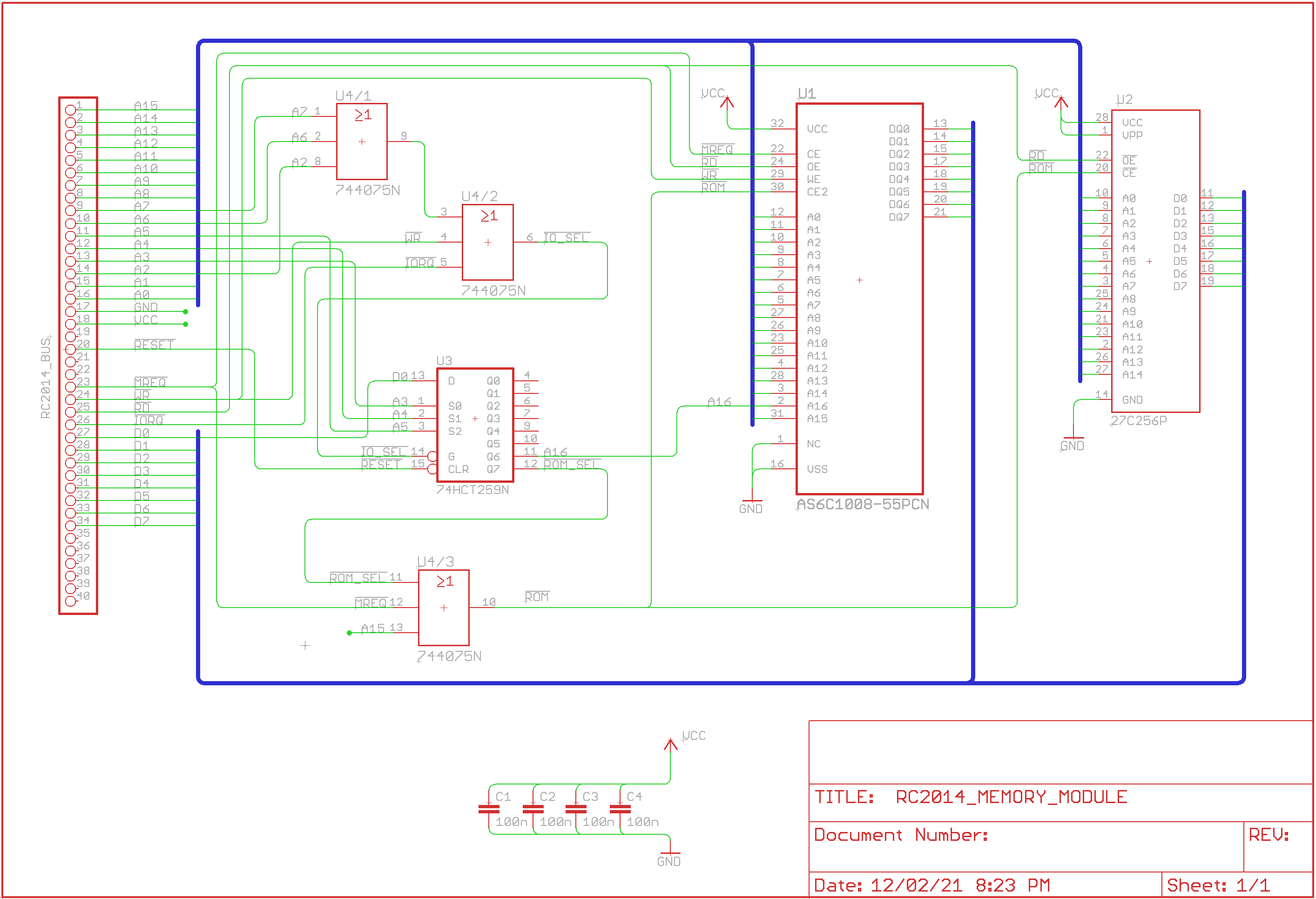
I guess the main feature is that it is really simple / cheap. Just 4 chips.
There are no jumpers or selectors. Super simple. Super cheap.
You get 32kB ROM at 0x0000, which can be paged out at address 0x38.
There are 2 banks of 64kB RAM, switchable at 0x30.
Basically, the design is cribbed from the SC114, but without any frills.
This functionality covers most of the standard ROMs, and this is the only use case I have. Pictures attached. Once proven I'll update this thread.
Cheers, Phillip

karlab
Feb 12, 2021, 6:48:17 AM2/12/21
to RC2014-Z80
Hi Phil.
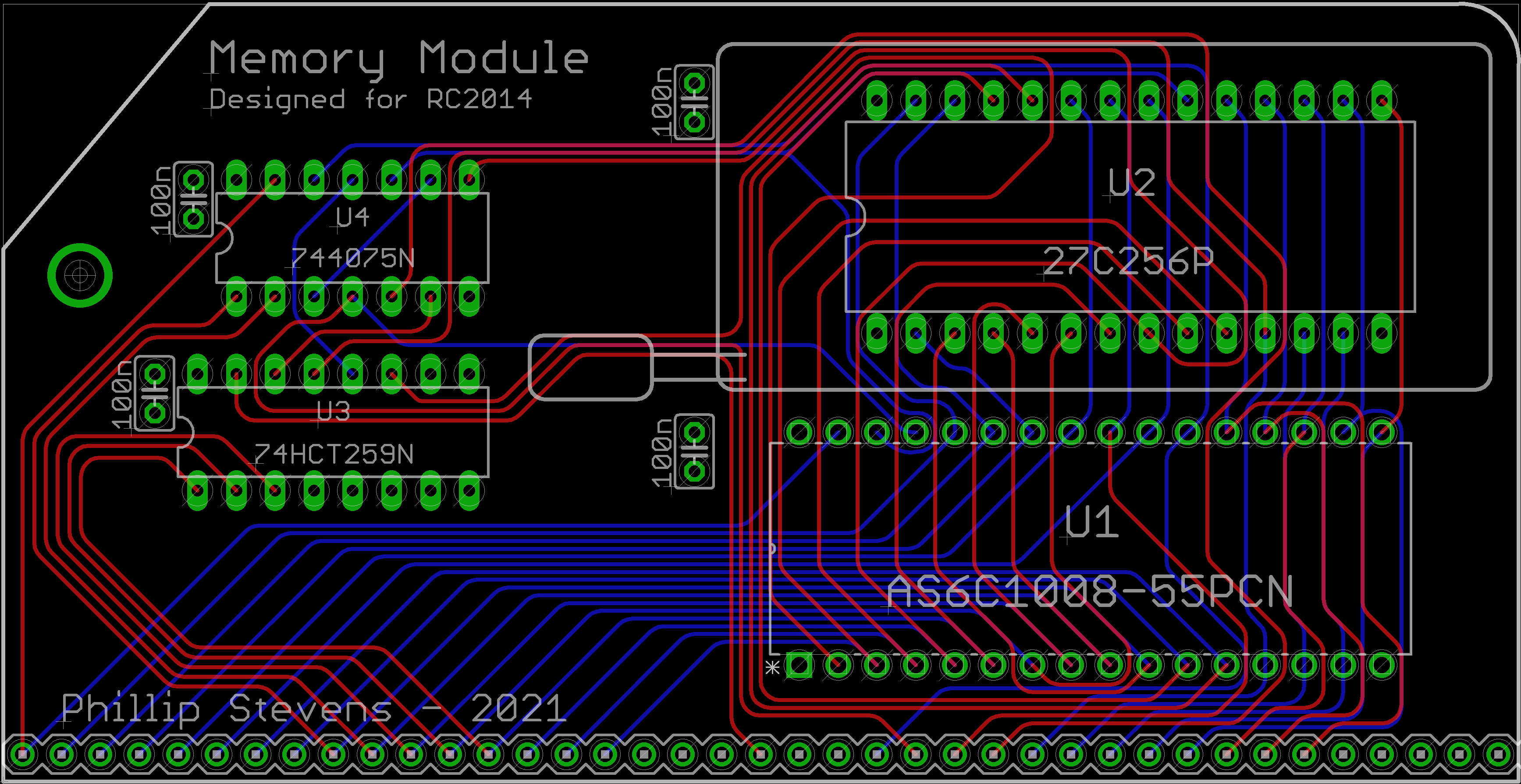
The traces on the PCB are beautiful.
Do you do the tracing manually?
Karl
Phillip Stevens
Feb 12, 2021, 7:01:50 AM2/12/21
to RC2014-Z80
karlab wrote:
The traces on the PCB are beautiful.Do you do the tracing manually?
Thanks Karl.
Yes I do them manually. It is sort of a karma inducing "join the dots" game for me.
Usually I'll start a few times, moving the components around, before finding the right flow for the board.
And, I'm always trying for the 0-via outcome.
Cheers, Phillip

Mark T
Feb 12, 2021, 2:09:08 PM2/12/21
to RC2014-Z80
Hi phillip,
Just curious if you tried rearranging the address lines to the ‘259, does it simplify the routing or just screw it up on the outputs? Sometimes it simplifies the routing with decoders or multiplexers, sometimes it messes it up more on the outputs.
Mark

Wesley Isacks
Feb 12, 2021, 6:45:25 PM2/12/21
to RC2014-Z80
I concur, the trace routing is lovely! I feel the same way about manual routing - it's almost meditative. I'm sure my tune would change if I had to do it every day, though.
-Wesley
Phillip Stevens
Feb 12, 2021, 9:52:37 PM2/12/21
to RC2014-Z80
Mark T wrote:
Just curious if you tried rearranging the address lines to the ‘259, does it simplify the routing or just screw it up on the outputs? Sometimes it simplifies the routing with decoders or multiplexers, sometimes it messes it up more on the outputs.
Hi Mark,
It turns out that keeping the addressing on the '259 wasn't hard to route, so I didn't think to change it. But, if it would have meant using a via I probably would have changed it, because karma.
If you know the AS5C1008, you'd note that the address lines have been optimised for layout karma though.
When thinking about this Module, I was looking to try to get the simplest and cheapest solution for supporting CP/M and the standard MS Basic builds. I think Steve has nailed it with the SC114 design. I spent a few hours looking for alternatives, like a 64kB RAM device (doesn't exist, afaik) or better 74' logic options, but couldn't find any.
Then, given that the '4075 has so many free latches, I started piling on some tri-colour LEDS, and some output pins. But then I slept on it and realised that it was not the original design goal, so I ripped all that out and went back to the bare minimum.
I still think it would be nice, and possible, to make the RAM into 32kB pages. But if I'm not mistaken that would add a bit more logic to the A15 addressing. So I discarded that idea too. Perhaps it is worth coming back to at some stage.
Cheers, Phillip
Wesley Isacks
Feb 12, 2021, 11:30:24 PM2/12/21
to RC2014-Z80
I'm working on 32K RAM pages next! Will post when I have something working.
-Wesley
Phillip Stevens
Feb 13, 2021, 2:44:14 AM2/13/21
to RC2014-Z80
I've been thinking about a method to use the additional 64kB of shadow RAM which will be available in Wesley and my new Modules, and also for those that have one of Steve's SC114 boards. Those solution that have a shadow RAM toggle at 0x30 (though it could be any register as needed).
As we have no RAM in a common area, the only way that I can think that this would work would be to have a code fragment stored by the bootloader in both of the RAM 64kB pages.
This would allow RAM to be copied back and forward across the whole address range, except the section where the code fragment exists of course.
I've mocked up some relocatable code and it is only 0x18 Bytes, so it would (for example) fit between the INT 0x38 and the NMI 0x66 addresses. Or, it could be copied into the shadow RAM CP/M FCB, and then loaded into the working RAM CP/M FCB just before it was needed. Lot's of options of where to put it.
I would have liked to make 64kB copies an option, but the overhead is too much in my opinion. It is better to divide up a copy into 256 Byte chunks in C, and do it that way. That preserves performance for small structure copies, and for floating point or other smaller copies.
The only caveat is that the same code has to be in both RAM banks in the same location, otherwise the PC will get borked and writing code to resolve that is beyond me.
Anyway, this is the guts of what I can put into z88dk so that all the shadow ram can be used from C.
12 0000 ; HL is the source address
13 0000 ; DE is the destination address
14 0000 ; B is the number of bytes to copy
15 0000
16 0000 ; Assemble with z88dk for RC2014 BASIC
17 0000 ; zcc +rc2014 -subtype=basic -v -m --list ramcopy.asm -o ramcopy -create-app
18 0000
19 0000 defc RAM_TOGGLE = $0030 ; The RAM bank is toggled by outputing 1/0 to 0x0030
20 0000
21 0000 PHASE 0x0040
22 0040
23 0040 .shadowcopy ;
24 0040 37 scf ; set our banks in reverse (more general if ccf used)
25 0041 17 rla ; carry to bit 0
26 0042 D3 30 out (RAM_TOGGLE),a ; now in other bank
27 0044 1F rra ; recover carry
28 0045
29 0045 .ramcopy
30 0045 7E ld a,(hl) ; get the byte
31 0046 23 inc hl
32 0047
33 0047 3F ccf ; toggle bank
34 0048 17 rla ; carry to bit 0
35 0049 D3 30 out (RAM_TOGGLE),a ; now in other bank
36 004B 1F rra ; recover carry and byte
37 004C
38 004C 12 ld (de),a ; store the byte
39 004D 13 inc de
40 004E
41 004E 3F ccf ; toggle bank
42 004F 17 rla ; carry to bit 0
43 0050 D3 30 out (RAM_TOGGLE),a ; now in other bank
44 0052 1F rra ; recover carry and byte
45 0053
46 0053 10 F0 djnz ramcopy ; decrement B
47 0055
48 0055 AF xor a ; get to front bank
49 0056 D3 30 out (RAM_TOGGLE),a ; now in front bank
50 0058 C9 ret
51 0059
52 0059 DEPHASE
53 0019
Any thoughts on how to do this better / another way?
Cheers, Phillip
Phillip Stevens
Feb 13, 2021, 2:56:28 AM2/13/21
to RC2014-Z80
I've been thinking about a method to use the additional 64kB of shadow RAM which will be available in Wesley and my new Modules, and also for those that have one of Steve's SC114 boards. Those solution that have a shadow RAM toggle at 0x30 (though it could be any register as needed).
I would have liked to make 64kB copies an option, but the overhead is too much in my opinion. It is better to divide up a copy into 256 Byte chunks in C, and do it that way. That preserves performance for small structure copies, and for floating point or other smaller copies.
This does up to 64kB copies. Not too much overhead either...
12 0000 ; HL is the source address
13 0000 ; DE is the destination address
14 0000 ; BC is the number of bytes to copy
15 0000
16 0000 ; Assemble with z88dk for RC2014 BASIC
17 0000 ; zcc +rc2014 -subtype=basic -v -m --list ramcopy.asm -o ramcopy -create-app
18 0000
19 0000 defc RAM_TOGGLE = $0030 ; The RAM bank is toggled by outputing 1/0 to 0x0030
20 0000
21 0000 PHASE 0x0040
22 0040
23 0040 .shadowcopy ;
24 0040 37 scf ; set our banks in reverse
25 0041 17 rla ; carry to bit 0
26 0042 D3 30 out (RAM_TOGGLE),a ; now in other bank
27 0044 1F rra ; recover carry
28 0045
29 0045 .ramcopy
30 0045 78 ld a,b ; swap BC to use cheap djnz
31 0046 41 ld b,c
32 0047 4F ld c,a
33 0048 03 inc bc ; make sure MSB in C is non-zero (without affecting carry)
34 0049
35 0049 .copyloop
36 0049 7E ld a,(hl) ; get the byte
37 004A 23 inc hl
38 004B
39 004B 3F ccf ; toggle bank
40 004C 17 rla ; carry to bit 0
41 004D D3 30 out (RAM_TOGGLE),a ; now in other bank
42 004F 1F rra ; recover carry and byte
43 0050
44 0050 12 ld (de),a ; store the byte
45 0051 13 inc de
46 0052
47 0052 3F ccf ; toggle bank
48 0053 17 rla ; carry to bit 0
49 0054 D3 30 out (RAM_TOGGLE),a ; now in other bank
50 0056 1F rra ; recover carry
51 0057
52 0057 10 F0 djnz copyloop ; decrement LSB
53 0059
54 0059 0D dec c ; decrement MSB
55 005A 20 ED jr NZ,copyloop
56 005C
57 005C AF xor a ; get to front bank
58 005D D3 30 out (RAM_TOGGLE),a ; now in front bank
59 005F C9 ret
60 0060
61 0060 DEPHASE

Steve Cousins
Feb 13, 2021, 4:58:08 AM2/13/21
to RC2014-Z80
Hi Phillip
As others have said, your board is a true work of art. I'm really impressed with the zero via implementation. I never seem to get close to that.
I use the same memory control circuit on several of my designs. I was unable to find a cheaper and/or lower chip count solution. To support this scheme I included an API in SCM v1.1 to allow a single byte to be written to or read from the second RAM page. This is limited to the top half of memory but enables bootstrap code to be copied over.
Steve

Alan Cox
Feb 13, 2021, 8:34:19 AM2/13/21
to rc201...@googlegroups.com
On Sat, 13 Feb 2021 at 07:44, Phillip Stevens <phillip...@gmail.com> wrote:
I've been thinking about a method to use the additional 64kB of shadow RAM which will be available in Wesley and my new Modules, and also for those that have one of Steve's SC114 boards. Those solution that have a shadow RAM toggle at 0x30 (though it could be any register as needed).As we have no RAM in a common area, the only way that I can think that this would work would be to have a code fragment stored by the bootloader in both of the RAM 64kB pages.This would allow RAM to be copied back and forward across the whole address range, except the section where the code fragment exists of course.
Fuzix on these boards uses a small piece of code in the ROM to bootstrap copying common helper code into both banks, which then works pretty much as you describe. It's a shade more complicated because it self modifies for speed and has to self modify the right bits in the right bank. There is a method in SCM for bank to bank copy, but because of the way things work out I can't actually use it directly and Fuzix ends up scanning the ROM to find it and call it directly - which works out fine.
My CP/M port for the fixed Simple80 (the original board has a bug) also supports using the second bank as a RAMdisc for CP/M in a similar way, as does my generic CP/M ROM. It's possibly not useful because the CF adapter is faster than bank switching copy 8)
Alan
Phillip Stevens
Feb 13, 2021, 8:55:37 AM2/13/21
to RC2014-Z80
I've been thinking about a method to use the additional 64kB of shadow RAM which will be available in Wesley and my new Modules, and also for those that have one of Steve's SC114 boards. Those solution that have a shadow RAM toggle at 0x30 (though it could be any register as needed).As we have no RAM in a common area, the only way that I can think that this would work would be to have a code fragment stored by the bootloader in both of the RAM 64kB pages.This would allow RAM to be copied back and forward across the whole address range, except the section where the code fragment exists of course.
Fuzix on these boards uses a small piece of code in the ROM to bootstrap copying common helper code into both banks, which then works pretty much as you describe. It's a shade more complicated because it self modifies for speed and has to self modify the right bits in the right bank. There is a method in SCM for bank to bank copy, but because of the way things work out I can't actually use it directly and Fuzix ends up scanning the ROM to find it and call it directly - which works out fine.
My CP/M port for the fixed Simple80 (the original board has a bug) also supports using the second bank as a RAMdisc for CP/M in a similar way.
Alan,
What mechanism did you use to hold the bank status?
Did you publish your Simple80 code?
I think using the carry bit to carry bank status works well as it isn’t affected by loop counting, and is relatively fast to recover without using a register. It will support 8080 too.
But there is probably a better way that I’ve overlooked entirely. Very open to suggestions.
P.

Bill Shen
Feb 13, 2021, 10:44:53 AM2/13/21
to RC2014-Z80
In Simple80, R16 needs to be pulled down rather than pulled up as in the original schematic.
https://www.retrobrewcomputers.org/doku.php?id=builderpages:plasmo:simple80
Alan and I have talked about copying data into all Z80 registers, including the alternate registers then switch bank and move data from registers to new bank. Because there are several Simple80 boards out there, I did not correct the design mistake but wrote a non-banked version of CP/M3 instead.
Bill
Alan Cox
Feb 13, 2021, 1:09:13 PM2/13/21
to rc201...@googlegroups.com
What mechanism did you use to hold the bank status?
Not sure I understand the question
- In general I know the bank because I have a bank "variable" I patch to be different in each bank copy, so a simple load of the address tells you
- In a copier you don't need to know because the two halves of the code being executed as it bounces bank to bank can be different anyway (and you can have to/from copiers). For a ramdisc
you also probably want a 128byte fixed size copier (especially for 8080 and 8085)
Did you publish your Simple80 code?
The non optimised one I used is, but the optimized one I forgot never got merged because I support SC108 and SC114 on the same kernel and never got around to a nice copier for both models. Those are in the Fuzix repository on github, and the universal CP/M ROM is in RC2014ROM repository (both github.com/EtchedPixels)
I will need to dig for the optimized one but basically it patches the out statements saving the re-use of the bc/de registers and uses de not ix. A truely optimized version (especially for 8080) would need to use the stack pointer.
Phillip Stevens
Feb 13, 2021, 9:12:04 PM2/13/21
to RC2014-Z80
Phillip wrote:I've been thinking about a method to use the additional 64kB of shadow RAM which will be available in Wesley and my new Modules, and also for those that have one of Steve's SC114 boards. Those solution that have a shadow RAM toggle at 0x30 (though it could be any register as needed).As we have no RAM in a common area, the only way that I can think that this would work would be to have a code fragment stored by the bootloader in both of the RAM 64kB pages.This would allow RAM to be copied back and forward across the whole address range, except the section where the code fragment exists of course.
Alan wrote:
Fuzix on these boards uses a small piece of code in the ROM to bootstrap copying common helper code into both banks, which then works pretty much as you describe. It's a shade more complicated because it self modifies for speed and has to self modify the right bits in the right bank.
Thanks Alan, Bill,
Good to hear I'm on the right track, and a code fragment in both banks at the same PC is necessary. I've found the code in Fuzix file sc108.s.
There is a method in SCM for bank to bank copy, but because of the way things work out I can't actually use it directly and Fuzix ends up scanning the ROM to find it and call it directly - which works out fine.
In the SCC v1.1 code I only find information which indicates that the shadow RAM is not implemented.
In SCC v1.23 I find following.
; **********************************************************************
; Read from banked RAM
; On entry: DE = Address in secondary bank
; On exit: A = Byte read from RAM
; F BC DE HL not specified
; IX IY I AF' BC' DE' HL' preserved
H_RdRAM: LD C,kBankPrt ;Bank select port address
LD B,1 ;Make B=1
OUT (C),B ;Select secondary RAM bank
LD A,(DE) ;Read from RAM
DEC B ;Make B=0
OUT (C),B ;Select primary RAM bank
RET
; **********************************************************************
; Write to banked RAM
; On entry: A = Byte to be written to RAM
; DE = Address in secondary bank
; On exit: AF BC DE HL not specified
; IX IY I AF' BC' DE' HL' preserved
H_WrRAM: LD C,kBankPrt ;Bank select port address
LD B,1 ;Make B=1
OUT (C),B ;Select secondary RAM bank
LD (DE),A ;Write to RAM
DEC B ;Make B=0
OUT (C),B ;Select primary RAM bank
RET
And the ROM to RAM API looks like this.
; **********************************************************************
; Copy from banked ROM to RAM
; On entry: A = ROM bank number (0 to n)
; HL = Source start address (in ROM)
; DE = Destination start address (in RAM)
; BC = Number of bytes to copy
; On exit: AF BC DE HL not specified
; IX IY I AF' BC' DE' HL' preserved
H_CopyROM: LDIR ;Only one bank so just copy memory
RET
So, I'd like take the H_CopyROM API as a given, since it is also used by LDIR. with a small clarification around A register.
and make a H_CopyRAM API suggestion.
; On entry: Interrupts disabled unless you know better
; A = Source RAM bank (0 / 1)
; HL = Source start address (in ROM)
; DE = Destination start address (in RAM)
; BC = Number of bytes to copy
; On exit: AF BC DE HL not specified
; IX IY I AF' BC' DE' HL' preserved
Depending on the space available, it might be best to do the BC shuffle and MSB increment in the calling functions. Though to keep things consistent I hope to do it in the copied code fragment. I'll see what comes out, and where the fragment can fit nicely.
Also, interrupts need to be stored and disabled, which can be best done in the calling C functions. Assembly programmers can look after it for themselves.
3 0000 SECTION code_user
4 0000
5 0000 PUBLIC shadowcopy
6 0000
10 0000 ; On entry: Interrupts disabled unless you know better
11 0000 ; A = Source RAM bank (0 / 1)
12 0000 ; HL = Source start address (in ROM)
13 0000 ; DE = Destination start address (in RAM)
14 0000 ; BC = Number of bytes to copy
15 0000 ; On exit: AF BC DE HL not specified
16 0000 ; IX IY I AF' BC' DE' HL' preserved
17 0000
21 0000 defc RAM_TOGGLE = $0030 ; The RAM bank is toggled by outputting 1/0 to 0x0030
22 0000
23 0000 PHASE 0x0050
24 0050
25 0050 .shadowcopy
26 0050 D3 30 out (RAM_TOGGLE),a ; now in other bank
27 0052 1F rra ; move current bank to carry
28 0053
29 0053 78 ld a,b ; swap BC to use cheap djnz
30 0054 41 ld b,c
31 0055 4F ld c,a
32 0056 0C inc c ; make sure MSB in C is non-zero (without affecting carry)
33 0057
34 0057 .copyloop
35 0057 7E ld a,(hl) ; get the byte
36 0058 23 inc hl
37 0059
38 0059 3F ccf ; toggle bank
39 005A 17 rla ; carry to bit 0
40 005B D3 30 out (RAM_TOGGLE),a ; now in other bank
41 005D 1F rra ; recover carry and byte
42 005E
43 005E 12 ld (de),a ; store the byte
44 005F 13 inc de
45 0060
46 0060 3F ccf ; toggle bank
47 0061 17 rla ; carry to bit 0
48 0062 D3 30 out (RAM_TOGGLE),a ; now in other bank
49 0064 1F rra ; recover carry
50 0065
51 0065 10 F0 djnz copyloop ; decrement LSB (without affecting carry)
52 0067
53 0067 0D dec c ; decrement MSB (without affecting carry)
54 0068 20 ED jr NZ,copyloop
55 006A
56 006A AF xor a ; get to front bank
57 006B D3 30 out (RAM_TOGGLE),a ; now in front bank
58 006D C9 ret
59 006E
60 006E DEPHASE
If the fragment exists in ROM only, then the top 32kB of shadow ram can be used.
If the fragment is copied on initialisation into both RAM banks (say somewhere in Page 0) then the whole 64kB of shadow RAM can be used.
Getting fancy would be to treat the shadow RAM as an additional C heap, and write malloc() and free() functions for it... but that's for another day.
P.
Alan Cox
Feb 13, 2021, 10:17:22 PM2/13/21
to rc201...@googlegroups.com
Also, interrupts need to be stored and disabled, which can be best done in the calling C functions. Assembly programmers can look after it for themselves.
I made my interrupt handlers save/restore the bank but that's probably overkill for a CP/M setup
Alan
Phillip Stevens
Feb 15, 2021, 3:27:15 AM2/15/21
to RC2014-Z80
Phillip wrote:
I've been thinking about a method to use the additional 64kB of shadow RAM which will be available in Wesley and my new Modules, and also for those that have one of Steve's SC114 boards. Those solution that have a shadow RAM toggle at 0x30 (though it could be any register as needed).
Spencer,
I think there's an issue with us using the 0x30 (or 48 in decimal) port to toggle the 64kB RAM pages because your Paged ROM Module also does something else with that port.
What did you design to happen when out (48),0 or out (48),1 are issued?
I might need to add a configuration to ensure that the data section asm_shadowcopy load preparation from ROM is only done if so configured.
Cheers, Phillip

Spencer Owen
Feb 15, 2021, 1:49:33 PM2/15/21
to rc201...@googlegroups.com
On Mon, 15 Feb 2021 at 08:27, Phillip Stevens <phillip...@gmail.com> wrote:
I think there's an issue with us using the 0x30 (or 48 in decimal) port to toggle the 64kB RAM pages because your Paged ROM Module also does something else with that port.What did you design to happen when out (48),0 or out (48),1 are issued?I might need to add a configuration to ensure that the data section asm_shadowcopy load preparation from ROM is only done if so configured.Cheers, Phillip
Hi Phillip,
This was quite a few years ago, so my memory is a bit hazy, but the thinking behind that would be that additional 32k RAM pages plus a 32k ROM page could be used, where the additional RAM pages are selectable by sending additional OUT (56),0 commands. Sending an OUT (48),0 would reset the '393, and bringing you back to the ROM page - either for speed (to save cycling though all the other pages) or to come back to a known page in case you lose track.
With careful software use, 3 additional 32k pages can be connected directly to the '393, just making sure that the counter is only incremented to 0, 1, 2, 4 or 8. However, with something like a 4-to-16 decoder inbetween the '393 and the RAM, 16 pages can be accessed.
This is fairly academic, though, as I don't think anybody has used this (previously undiscussed) feature. Certainly the software side is beyond my abilities, and with RomWBW happily working with 512k ROM and 512k RAM, I'm not sure there is really much call for it.
Spencer
Phillip Stevens
Feb 15, 2021, 10:52:46 PM2/15/21
to RC2014-Z80
Phillip wrote:
I think there's an issue with us using the 0x30 (or 48 in decimal) port to toggle the 64kB RAM pages because your Paged ROM Module also does something else with that port.What did you design to happen when out (48),0 or out (48),1 are issued?
Spencer Owen wrote:
Sending an OUT (48),0 would reset the '393, and bringing you back to the ROM page - either for speed (to save cycling though all the other pages) or to come back to a known page in case you lose track.
This is fairly academic, though, as I don't think anybody has used this (previously undiscussed) feature.
Thanks for clarifying / confirming Spencer.
I had written half a page notes here, but then browser crash and, poof, gone.
Suffice to say that it is a pity that I didn't read your schematic or even my own code before proceeding, but it doesn't really matter in the end.
The user will just have to be aware of which memory type they are have when using the functions, or they will be bounced back to ROM.
For z88dk, it doesn't make a difference, since for both ROM builds (ACIA and SIO) the asm_shadowcopy relocatable code can be initialised into both (or twice into one) banks without any care.
The asm_shadowcopy code is assigned to the DATA section, so it will be automatically decompressed and located in RAM, along with the user's shadowwrite() and shadowread() functions.
In the builds I've been playing with, it happens to be the first thing in DATA, so is located at 0x8000. But that isn't guaranteed.
Then, using the functions so placed from ROM, it is possible to relocate them to any other RAM location as needed, with a bit of further juggling.
So I believe that's a memcpy()similar set of functions done, and ready for use with a SC108, SC114 or Wesley's rc-ramrom.
P.
Phillip Stevens
Mar 11, 2021, 7:50:05 PM3/11/21
to RC2014-Z80
Phillip Stevens wrote:
As mentioned, on other threads I just finished a very simple RAM/ROM Module.I guess the main feature is that it is really simple / cheap. Just 4 chips.There are no jumpers or selectors. Super simple.
You get 32kB ROM at 0x0000, which can be paged out at address 0x38.There are 2 banks of 64kB RAM, switchable at 0x30.Basically, the design is cribbed from the SC114, but without any frills.This functionality covers most of the standard ROMs, and this is the only use case I have.
Pictures attached. Once proven I'll update this thread.
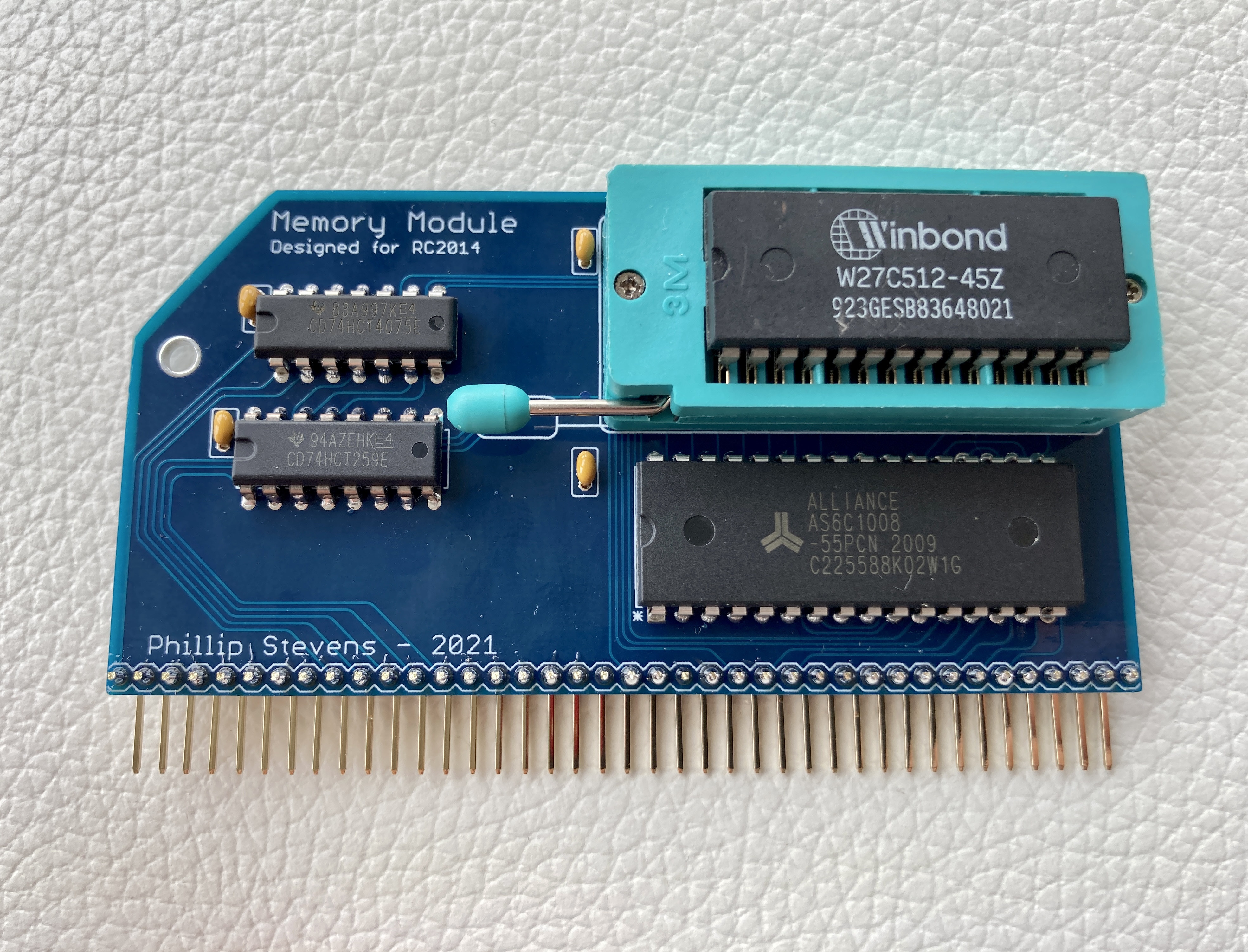
And, here's the update. I've build some up some of these PCBs and they work as intended.

The only issue was that the PCB manufacturer misunderstood my dimension instructions, and sent me rectangular PCBs.
I mean, what were they thinking?
One small advantage over separate ROM and RAM boards when using the standard Backplane 8, is that you don't need a separate flying /PAGE wire.
That's very convenient.
I've put my excess PCBs up on Tindie as the "Memory Module". I've five rectangular PCBs that need to be filed to shape. Use "REWORK" code to get them at $3.00.
As always, postage from AU is a PITA, so let me know if you'd like to make your own and I'll send the Gerber files.
Cheers, Phillip
Wesley Isacks
Mar 12, 2021, 6:35:22 PM3/12/21
to RC2014-Z80
Looking good! And I see you went for a 4-layer board, very nice.
I should list my extra boards on Tindie... I have quite a collection of them at this point. How hard is it to set up a store?
-Wesley
Phillip Stevens
Mar 12, 2021, 7:12:49 PM3/12/21
to RC2014-Z80
Wesley Isacks wrote:
Looking good! And I see you went for a 4-layer board, very nice.
Thanks.
I should list my extra boards on Tindie... I have quite a collection of them at this point. How hard is it to set up a store?
It is very easy to set up a store. Really you just have to describe what your product is.
The only background thing to do is to work out what your shipping rates are.
From AU it is pretty easy really to work out shipping rates. If you cross the water (i.e. outside AU), I can never get out of the Post Office for less than ~A$30.
Which is a real issue when you're selling a $3.00 item.
I've put my excess PCBs up on Tindie as the "Memory Module". I've five rectangular PCBs that need to be filed to shape. Use "REWORK" code to get them at $3.00.As always, postage from AU is a PITA, so let me know if you'd like to make your own and I'll send the Gerber files.
P.
Phillip Stevens
Mar 26, 2021, 12:48:12 AM3/26/21
to RC2014-Z80
As mentioned, on other threads I just finished a very simple RAM/ROM Module.I guess the main feature is that it is really simple / cheap. Just 4 chips.There are no jumpers or selectors. Super simple.You get 32kB ROM at 0x0000, which can be paged out at address 0x38.There are 2 banks of 64kB RAM, switchable at 0x30.Basically, the design is cribbed from the SC114, but without any frills.This functionality covers most of the standard ROMs, and this is the only use case I have.
The only issue was that the PCB manufacturer misunderstood my dimension instructions, and sent me rectangular PCBs.
One small advantage over separate ROM and RAM boards when using the standard Backplane 8, is that you don't need a separate flying /PAGE wire.That's very convenient.
The replacement RC2014 shaped PCBs have finally arrived, and they're listed on Tindie now.
I've put my PCBs up on Tindie as the "Memory Module".
While I've got some of the rectangular (electrically identical) PCBs left over, I'll throw them in one for one, with any orders.
As always, postage from AU is a PITA, so let me know if you'd like to make your own PCBs and I'll send you Gerber files.
Cheers, Phillip
Phillip Stevens
Sep 14, 2021, 6:37:45 AM9/14/21
to RC2014-Z80
I've reordered some more Memory Module PCBs for Tindie, which should arrive in a week or so.
But because postage from Australia is such an expensive PITA, I've also put the Memory Module up on Seeed Fusion so anyone can order the PCB from them directly.
Cheers, Phillip
Phillip Stevens wrote:
As mentioned, on other threads I just finished a very simple RAM/ROM Module.I guess the main feature is that it is really simple / cheap. Just 4 chips.There are no jumpers or selectors. Super simple.You get 32kB ROM at 0x0000, which can be paged out at address 0x38.There are 2 banks of 64kB RAM, switchable at 0x30.Basically, the design is cribbed from the SC114, but without any frills.This functionality covers most of the standard ROMs, and this is the only use case I have.The only issue was that the PCB manufacturer misunderstood my dimension instructions, and sent me rectangular PCBs.One small advantage over separate ROM and RAM boards when using the standard Backplane 8, is that you don't need a separate flying /PAGE wire.That's very convenient.

Phillip Stevens
May 7, 2022, 6:41:20 AM5/7/22
to RC2014-Z80
As I'm planning to be mainly unavailable for a longish while, and so my Tindie store will be on vacation more often than not, I've published the design on Seeed Studio Fusion.
The PCBs for the Memory Module can be ordered there, or the Gerber file used to order at your favourite PCB vendor.
Cheers, Phillip
As mentioned, on other threads I just finished a very simple RAM/ROM Module.I guess the main feature is that it is really simple / cheap. Just 4 chips.There are no jumpers or selectors.
You get 32kB ROM at 0x0000, which can be paged out at address 0x38.There are 2 banks of 64kB RAM, switchable at 0x30.Basically, the design is cribbed from the SC114, but without any frills.This functionality covers most of the standard ROMs, and this is the only use case I have.

Reply all
Reply to author
Forward
0 new messages