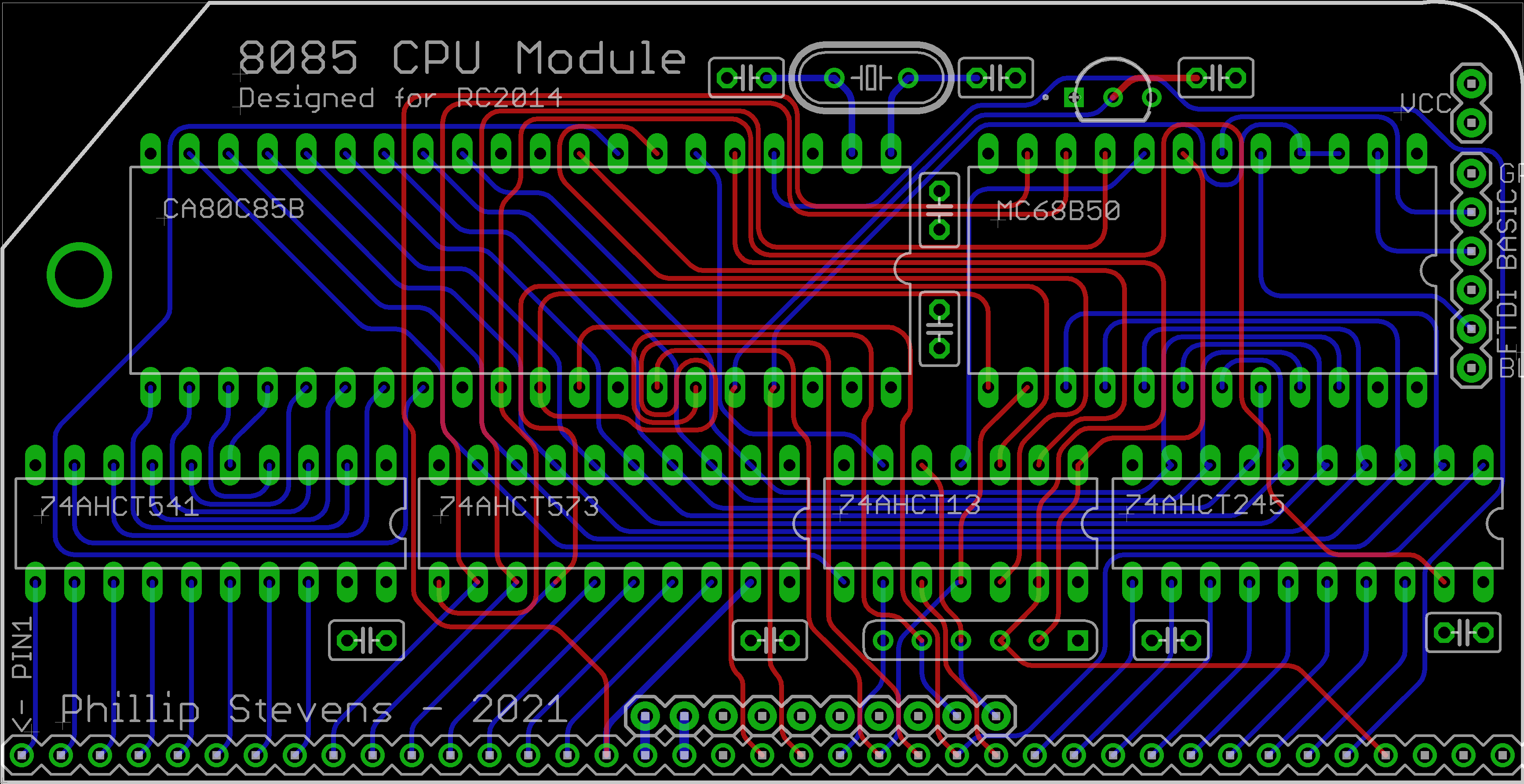
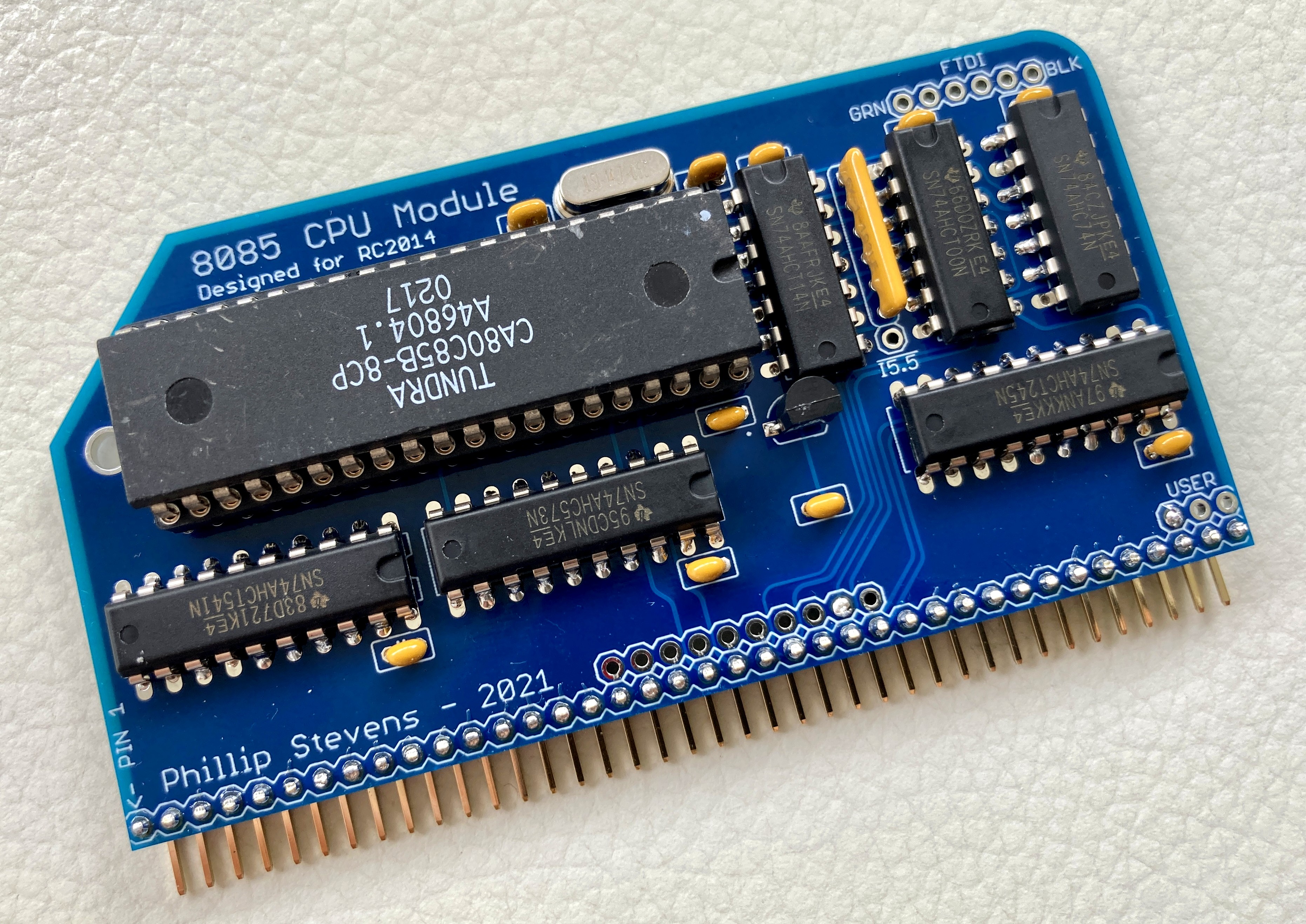
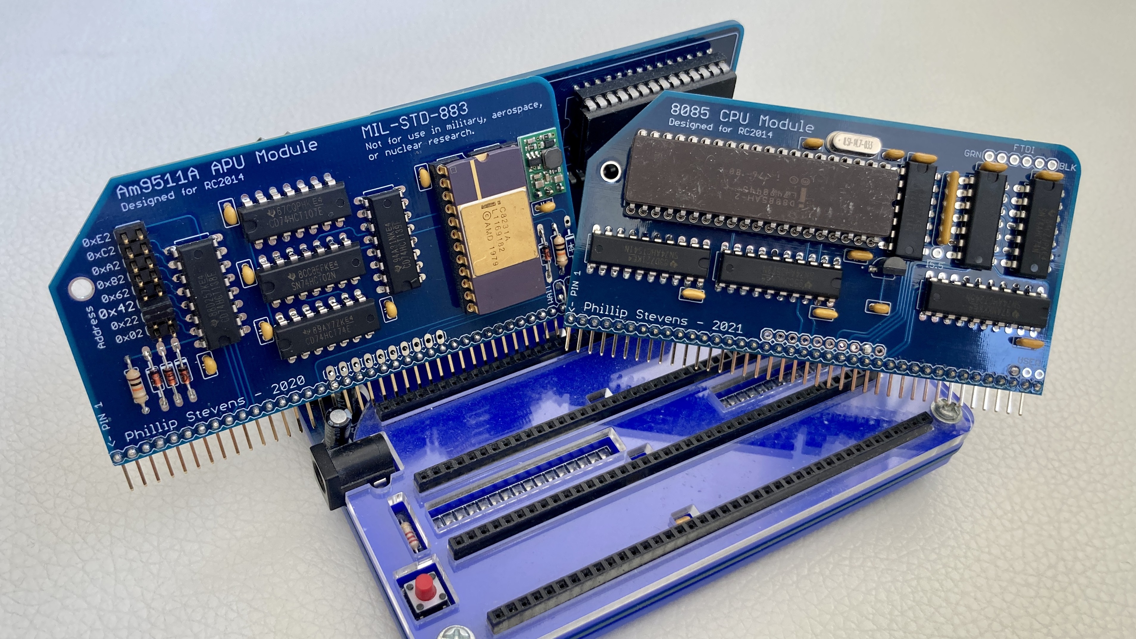
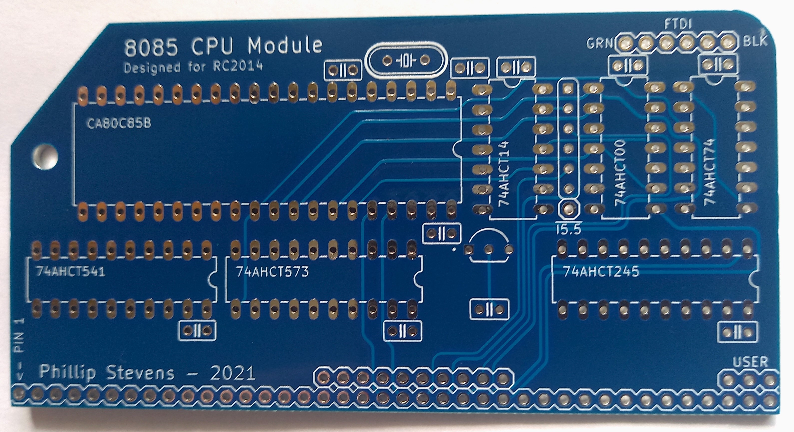
New 8085 CPU Module designed for RC2014

Phillip Stevens


Alan Cox
SInce the 8085 has no Mode 2 interrupt but has plenty of interrupt lines, I thought the best option was to put a MC6850 UART on the PCB. That way it could use one of the IM1 interrupts, and another interrupt could be directed to the RC2014 Bus. I've also set the SID/SOD pins up with another interrupt to allow them to be a second (slower) bit-banged UART, but with no flow control.It might be a while before this gets built up, but happy to share the build if someone would like the Gerbers.

Tadeusz Pycio
Alan's comment on the interrupts is important.
Phillip Stevens
Since the 8085 has no Mode 2 interrupt but has plenty of interrupt lines, I thought the best option was to put a MC6850 UART on the PCB. That way it could use one of the IM1 interrupts, and another interrupt could be directed to the RC2014 Bus. I've also set the SID/SOD pins up with another interrupt to allow them to be a second (slower) bit-banged UART, but with no flow control.
Looking at your design - you don't need the extra buffers if you have an 80C85 (you may well do for a classic 8085 if you have any 74LS/ALS on the backplane), and you will have problems with external interrupts because RST7_5 is edge triggered which is why it is normally used for the bitbang serial interrupt.
The one I designed and built (loosely based on Ben's original) is at
I have it running with a Tundra 80C85 at the standard 7.37MHz (8MHz 80C85 part). Except for it hating the CF adapter at that speed and the usual Z80 specific chips it seems to be rock solid.
Alan Cox
Is there a reason why the 7.5 interrupt is not the "best" interrupt and suitable to use on the RC2014 bus?
The one I designed and built (loosely based on Ben's original) is atYes, I saw your MMU version. I am trying to be a little simpler, and just use the existing memory modules for the RC2014, and just aiming for a 64kB CP/M solution.
I have it running with a Tundra 80C85 at the standard 7.37MHz (8MHz 80C85 part). Except for it hating the CF adapter at that speed and the usual Z80 specific chips it seems to be rock solid.Actually it was reading about the CF issues you faced in the post mentioned, and participating in the conversations elsewhere about issues with CF cards generally that lead me to use the AHCT logic bus buffers.
Got to admit that I don't even have a CF Module, preferring to use the 8255 IDE Module exclusively. But, I thought others might find it helpful though.Happy to hear that it is working well at 7.3MHz.The Tundra 80C85B suppliers that I've found are all eBay. Not sure I'd be getting the right thing buying there. But perhaps UTSource has some.

Bill Shen

Chris Odorjan
Happy to hear that it is working well at 7.3MHz.The Tundra 80C85B suppliers that I've found are all eBay. Not sure I'd be getting the right thing buying there. But perhaps UTSource has some.
Phillip Stevens
Is there a reason why the 7.5 interrupt is not the "best" interrupt and suitable to use on the RC2014 bus?All the existing hardware expects level triggered interrupt behaviour like the Z80 provides. Also for the serial you want the edge (inverted if I remember rightly) and the highest priority so that the bitbanger gets serviced fast. Same reason you wire the bitbanger to the NMI on a Z80.
The one I designed and built (loosely based on Ben's original) is at
Yes, I saw your MMU version. I am trying to be a little simpler, and just use the existing memory modules for the RC2014, and just aiming for a 64kB CP/M.
I have it running with a Tundra 80C85 at the standard 7.37MHz (8MHz 80C85 part). Except for it hating the CF adapter at that speed and the usual Z80 specific chips it seems to be rock solid.
If it's drive related - if it's timing related then it won't make any difference. I've not dug into the signal ordering in detail to double check. Of course if it's drive related you want the buffers on the CF end.
AHCT may also not be a good idea unless you have to - AHCT has very sharp edges and very sharp edges on a long passive unterminated bus with random slower logic all down it makes me nervous.
Phillip Stevens
Alan wrote:Is there a reason why the 7.5 interrupt is not the "best" interrupt and suitable to use on the RC2014 bus?All the existing hardware expects level triggered interrupt behaviour like the Z80 provides. Also for the serial you want the edge (inverted if I remember rightly) and the highest priority so that the bitbanger gets serviced fast. Same reason you wire the bitbanger to the NMI on a Z80.All fair points. I’ve redone the interrupt assignment to match yours.TRAP <- inverted NMI line.7.5 <- inverted RX line. For bit bang serial, and effectively a second interrupt.6.5 <- inverted INT line.5.5 <- inverted 6850 IRQ.INTR <- GND.
Alan Cox
Noted that you tie X2 capacitor high, rather than to GND as per datasheet. Is there a background to that decision?
I have it running with a Tundra 80C85 at the standard 7.37MHz (8MHz 80C85 part). Except for it hating the CF adapter at that speed and the usual Z80 specific chips it seems to be rock solid.If it's drive related - if it's timing related then it won't make any difference. I've not dug into the signal ordering in detail to double check. Of course if it's drive related you want the buffers on the CF end.Yes I think that was the summary of the other discussion too. But failing buffers on the standard CF Module, it can’t be worse to do it on CPU Module and the user can also just jumper over them if preferred.
Reading material suggests whilst AHCT is very fast, the drive (8mA) is much less than standard CMOS, and hence doesn’t tend to bounce. But how much is marketing, and how much is real, I don’t know. Not a hill to die on.
Phillip Stevens
Good news: The replacements (date codes in the late 1990s) work fine in an SBC I've built (that I need to document on retro-comp sometime) at 7.3728MHz without buffers. Admittedly it's a small board without expansion and the only things on the bus are the address latch, RAM, ROM/flash, a DUART, and an SPLD to glue everything together.
More good news: I've had good luck getting OKI MSM80C85AHRS CPUs and even ceramic-topped Intel 8085AH CPUs, both rated at 5MHz (and also obtained from Utsource) running reliably at 7.3728MHz. (I need to do some more testing and document.
Alan Cox
do you know how reliable is the presence of the undocumented instructions?I mean on Z80 the undocumented instructions are always present. But I read the 8085 undocumented instructions may not always be present, depending on the manufacturer build.The 8085B has them. Does the OKI device?
Phillip Stevens
As far as anyone has been able to test and verify 100%. From a compiler perspective it's a shame Intel did that as they fixed pretty much all the nasty 8080 code generation problems with a tiny number of rather elegantly designed instructions.Alan
Phillip Stevens
Over the past few days I've been reworking MS Basic 4.7 to make it 8085 clean (again).
Alan Cox
Phillip wrote:Over the past few days I've been reworking MS Basic 4.7 to make it 8085 clean (again).I have found what I believe to be an interesting piece of software archaeology.From what I can tell, MSBasic 4.7 was never 8080 / 85 clean.
Chris Odorjan
When assembling it tonight, I found a few Z80 instructions remaining scattered in the code.I know they were not my doing so I went back to the paper disassembly document and found that they're written in there too.They are ADC HL,DC and LD (**),DEI first thought that there might have been a transcription typo, and the intended instruction was ADD HL,DE but, because the P flag is later tested, the author meant to use ADC instruction.
Any guesses as to where and when these instructions came in to the code?
Phillip Stevens
Over the past few days I've been reworking MS Basic 4.7 to make it 8085 clean (again).I have found what I believe to be an interesting piece of software archaeology.From what I can tell, MSBasic 4.7 was never 8080 / 85 clean.4.7b (the one you have) was for the Nascom; it's entirely possible they had some Z80 specific tweaks. 4.51 was the last Microsoft Basic 4.x release for CP/M before the big changes in 5.0. The CP/M ones do support 8080.
Phillip Stevens
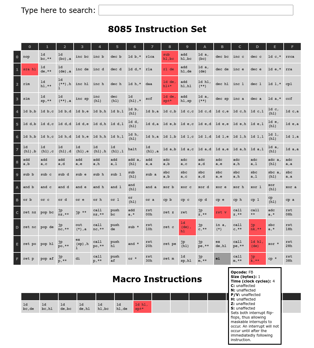
Because TASM didn't understand Zilog 8085 opcodes out of the box, I've made a table specifically for extended 8085 in Zilog with opcodes. This TASM85.TAB replaces the Intel 8085 version.
Alan Cox
Phillip wrote:Because TASM didn't understand Zilog 8085 opcodes out of the box, I've made a table specifically for extended 8085 in Zilog with opcodes. This TASM85.TAB replaces the Intel 8085 version.Does anyone know what the effect is of adding a 2s complement number in `LD DE,SP+n`?The assemblers all produce `$FF` if confronted with `LD DE,SP+-1`, but adding 255 to the SP is far less useful for high level languages than subtracting 128, and establishing a stack frame
Chris Odorjan
The text all seems to point to the offset being an unsigned number though. So, I’m now doubtful that they did the sensible thing.
Phillip Stevens
The text all seems to point to the offset being an unsigned number though. So, I’m now doubtful that they did the sensible thing.
I wondered this at some point in the past and kept the results of a test program (I think I was working on an 8085 emulator). It produced FEFF (when SP=FE00), not FDFF., so unfortunately it's unsigned.
On the other hand it doesn't affect flags, so something like XCHG; LDSI 0; XCHG will get SP in HL without clearing carry like LXI HL,0; DAD SP does (and in the same time and size).
Alan Cox
Alan, not sure I understand “The better 8080 C compilers already knew how to avoid the cost of a frame pointer so it makes a lot of sense to be unsigned.”?How did they calculate a stack relative address, without using SP as a pointer? I didn’t think there were enough registers free to use one as a frame pointer. Or, did they just use 8080/Z80 style push/pop to access stack variables?
Phillip Stevens
So this is what I'm going to mull on for a few days.It should be compatible with Alan's 8085 Module for interrupts, etc, so for the user it would just be a choice of integrated MMU, or integrated 6850 USART.But everything else should be the same.

 I
IAlan Cox
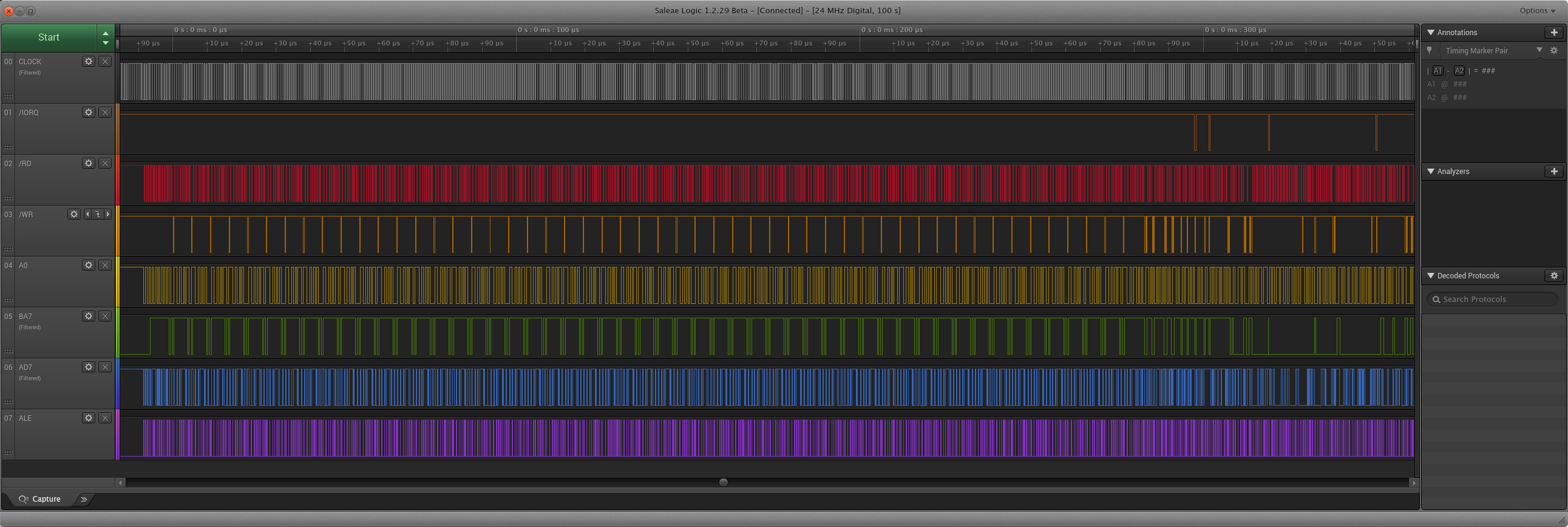
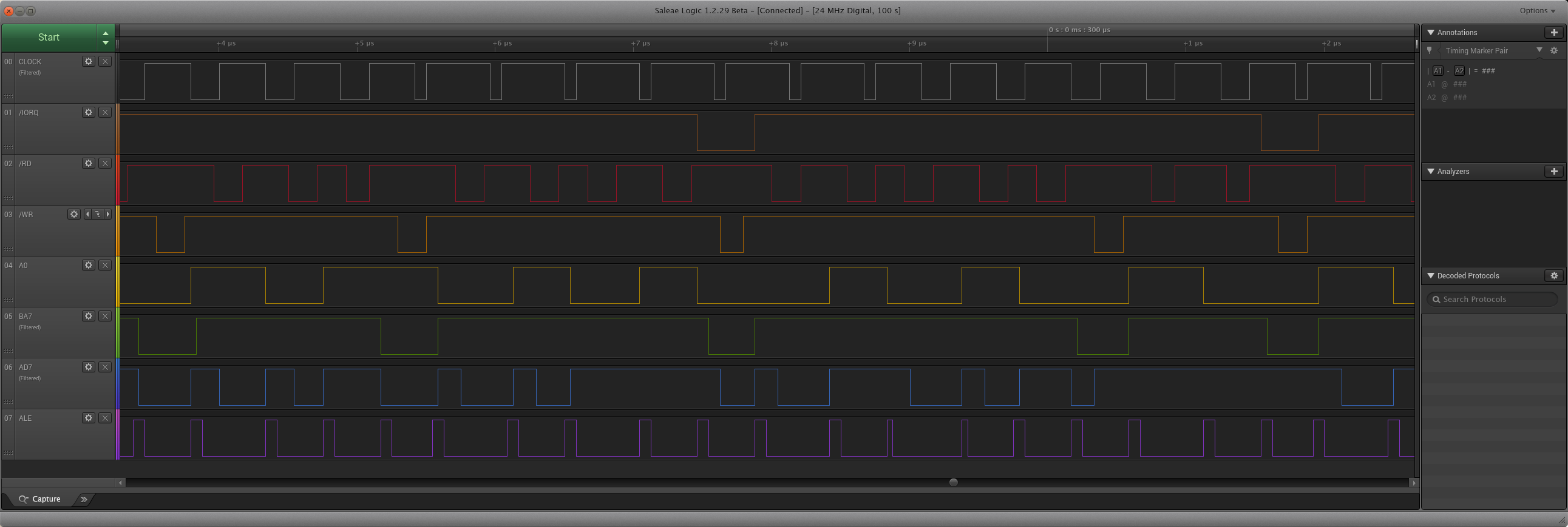
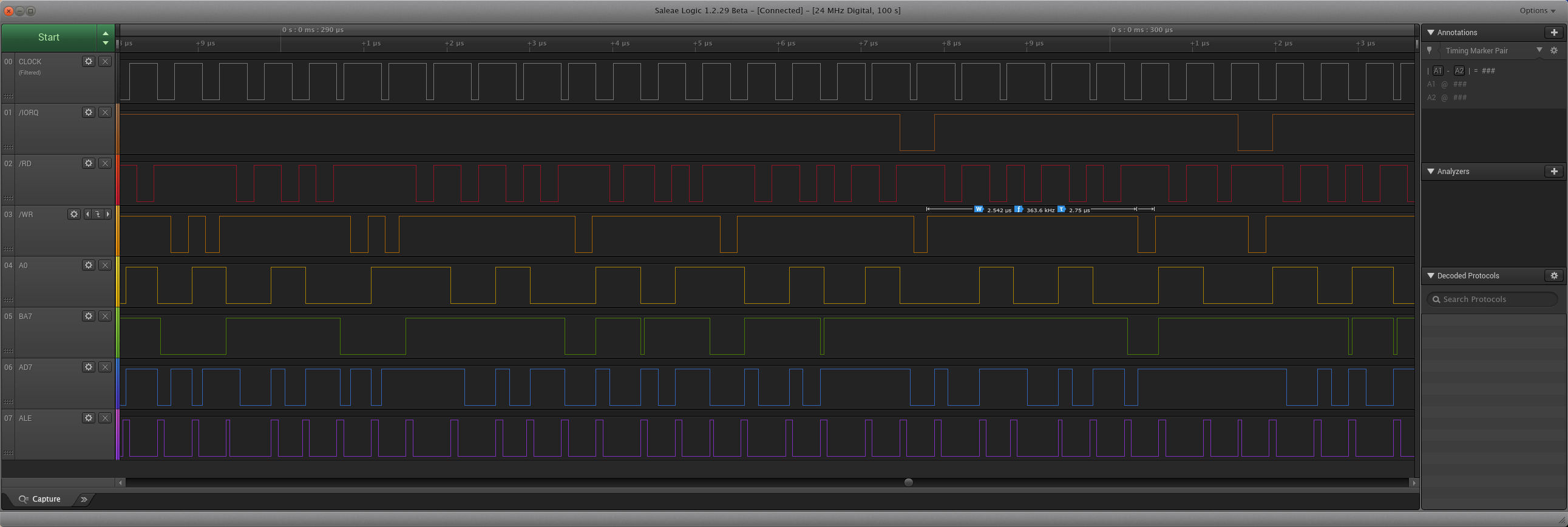
What I'm finding quite interesting (read bloody annoying) is that for every other read or write cycle the ALE correctly traps the address, and the BA7 line is correct.It is only when writing to /IORQ that it is going wrong. In fact on the second write to the 6850 the BA7 line goes out of its way to be wrong

Greg Holdren
Phillip Stevens
I think you need to do something with the G of the 245. There is bus contention on the internal databus between the 245 and the UART during read.
Alan wrote:Looking at the traces I may be missing something but I think your problem is the buffering logic is wrong. For a write cycle at least RD will stay high. Now with RD always high the74HCT245N will drive the RC2014 bus signals onto AD0-AD7 during the address demultiplexing cycles so the 74HCT573 actually sees a fight between the latch and the CPU.
What happens if you pull the '245 and replace it with 8 wire links?
Alan Cox
I would go so far as to say that, I can't see how a robust 8085 system can work without data bus isolation (a tristate transceiver like a '245).Without the isolation, any device on the bus can "wake up" its bus drivers when it sees its I/O address and the RD line, and disturb the data bus whilst the CPU is trying to latch these low addresses.
Phillip Stevens
I would go so far as to say that, I can't see how a robust 8085 system can work without data bus isolation (a tristate transceiver like a '245).Without the isolation, any device on the bus can "wake up" its bus drivers when it sees its I/O address and the RD line, and disturb the data bus whilst the CPU is trying to latch these low addresses.
RD does not go low until the rising clock edge in the middle of T2. So the device will not get an RD or WR until the point it has valid data on the bus for a write or is expected to provide it for a read. Your 68B50 is, however, Motorola bus so you are using \WR as R/W and that won't work because your E clock isn't properly qualified by requiring either \RD or \WR is low.
I still think your 245 setup looks wrong. During the T1 cycle the CPU drives AD0-AD7 with the address and DIR is \RD which is high so the 74HCT245 also drives the same lines with whatever is randomly floating about on the bus.
G needs to be something like a NAND of \RD and \WR so the buffer is only active when data is being transferred. Maybe you can just flip the sides of the HCT245 and use \WR so that the 245 drives the bus with crap during address demux cycles but you seem to need the same signal for the 68B50 anyway.
It's very different to the Z80 cycles where RD and MREQ/IORQ are basically aligned. On an 8085 your generated MREQ and IORQ occur much earlier and you will get spurious selects without RD/WR. That is fine with the proper decoding because they are no different to the glitches you get on the Z80 bus because they are not quite aligned, even more so once buffers or decoders are involved.
Phillip Stevens
Phillip wrote:I've attached the current broken schematic. I'm planning to move the 6850 data lines to the "outside" data bus. But the layout will be a pita I'm sure.But first I'm testing using an old 6850 RC2014 board and the IRQ6.5 to make sure that there's nothing else broken.
Updates when I've more test results.
Alan Cox
I don't think I posted the most recent schematic (there were too many changes). But on the built PCB I'm driving the '245 /OE input with the ALE pin. This disables the '245 outputs while ALE is high. The '573 only needs 1ns to latch the addresses when ALE falls, but the '245 takes typically 9ns to 14ns on /OE to reactivate either set of outputs. So the CPU now has a clean window to latch the low addresses no matter what sins are happening on the "outer bus".
Phillip Stevens
I don't have a functioning ACIA Module, and I can't repair my broken one with the new MC6850 devices.So until that is resolved, I've got nothing more I can do.
- ALE is only driven high during the low half cycle of T1, so for the second half of T1 and the first half of T2 whilst you've latched the data the CPU is fighting the 245 on the bus still. It's better but it still looks very wrong. You should only drive the AD lines into the CPU when \RD is low.
Phillip Stevens
But my code is not working with ACIA as it stands.
However, the 8085 module is working, and counts using digital I/O Module, etc. So I think the non-working ACIA is a combination of a) bad code b) possibly overclocking on subtlety on non B type 6850 c) possible timing issues d) IDK.
But the proposed method using the IO / /M line provided by the 8085 happens very early.
Alan Cox
But my code is not working with ACIA as it stands.However, the 8085 module is working, and counts using digital I/O Module, etc. So I think the non-working ACIA is a combination of a) bad code b) possibly overclocking on subtlety on non B type 6850 c) possible timing issues d) IDK.
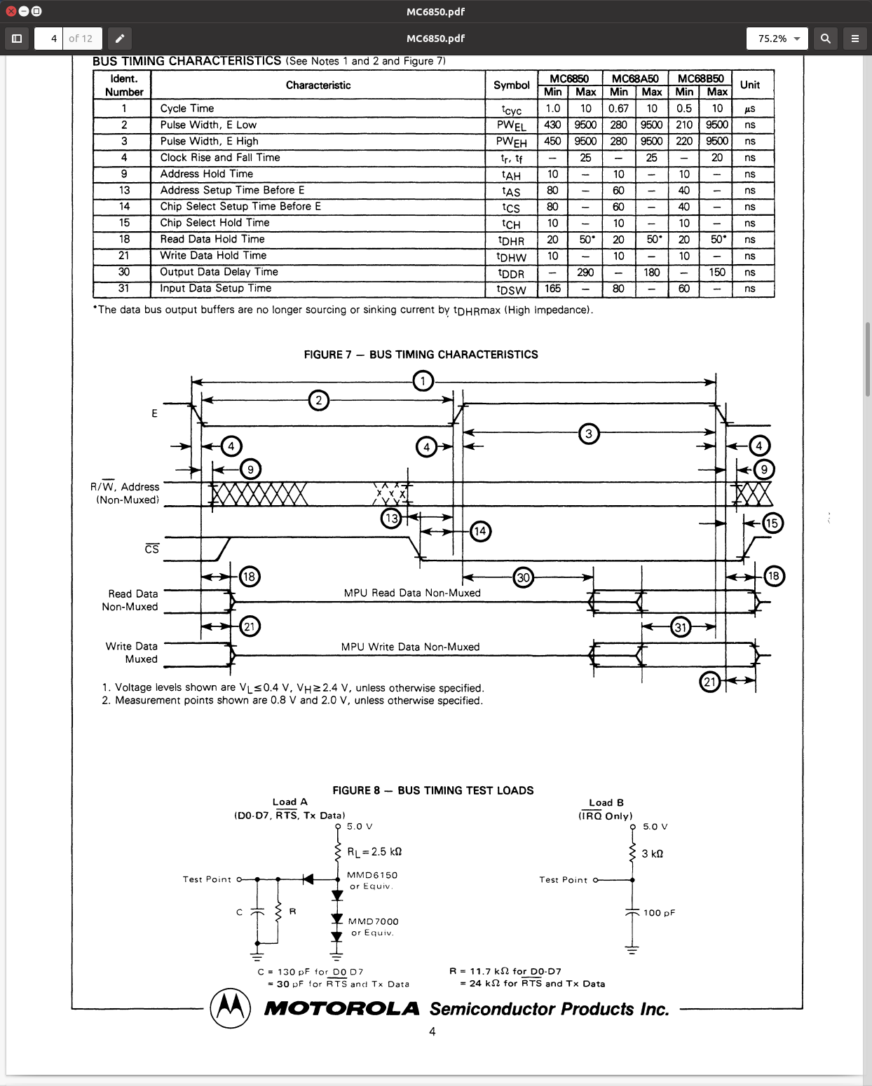
The 6850 needs the E signal to happen after the address and /CS lines have stabilised. 13 and 14 in below image.
But the proposed method using the IO / /M line provided by the 8085 happens very early.Even before the address lines have been stabilised. This is clearly wrong.
Phillip Stevens
But my code is not working with ACIA as it stands.However, the 8085 module is working, and counts using digital I/O Module, etc.
So I think the non-working ACIA is a combination of a) ... b) ... c) possible timing issues d) ...
The 6850 needs the E signal to happen after the address and /CS lines have stabilised.
But the proposed method using the IO / /M line provided by the 8085 happens very early.
Even before the address lines have been stabilised. This is clearly wrong.
I think it's "one of RD or WR low". Z80 you can get away with IORQ as E generally.
I think the result can be obtained in 4 NAND gates, which fits into a 7400 nicely.
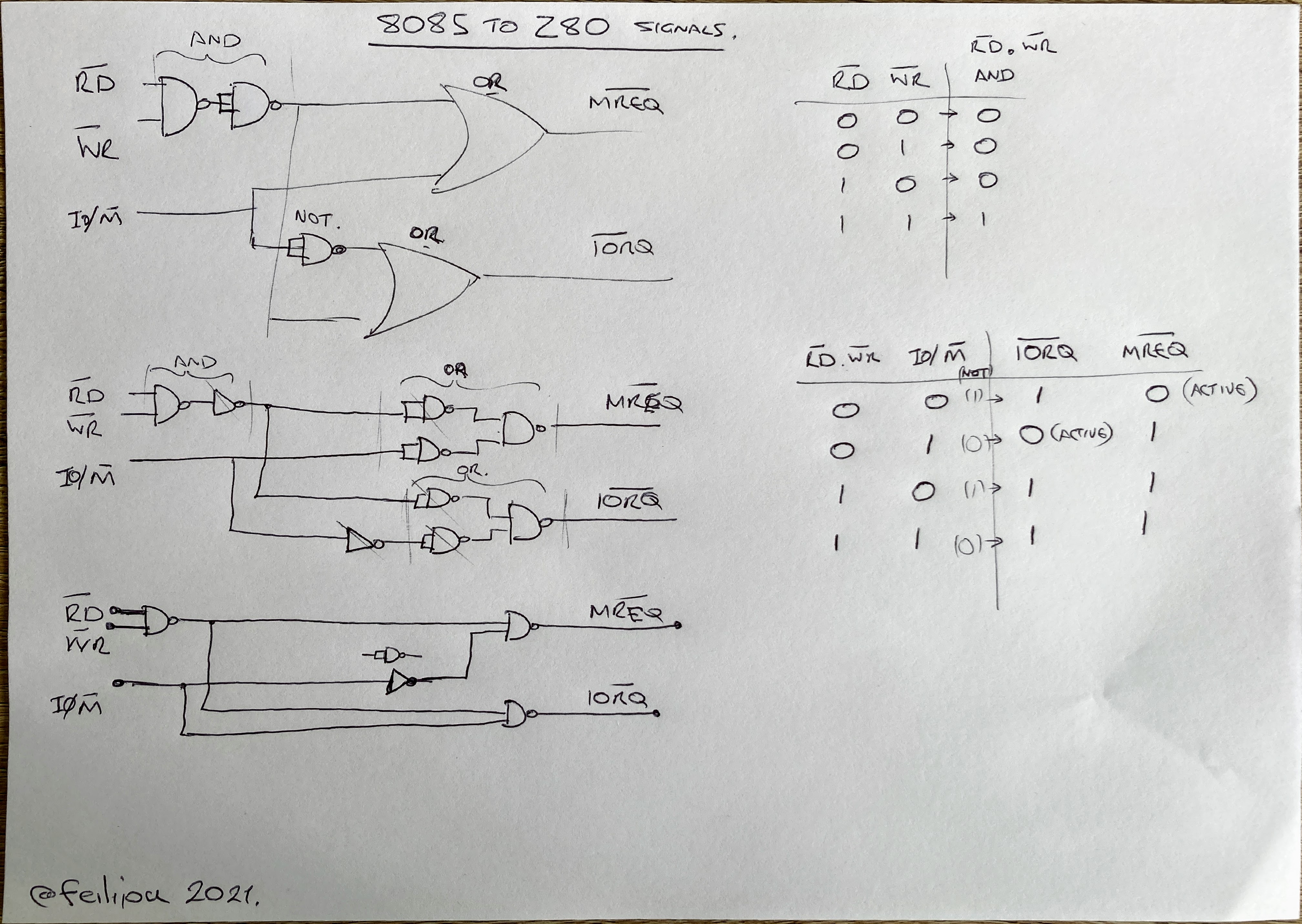
If you generate IORQ that way for the bus however it would make the access times much shorter and I don't know what that would result in.
I can confirm the undoctored 68B50 doesn't work with my 8085 card either though.
Phillip Stevens
Phillip Stevens
On the other hand it doesn't affect flags, so something like XCHG; LDSI 0; XCHG will get SP in HL without clearing carry like LXI HL,0; DAD SP does (and in the same time and size).
Phillip Stevens
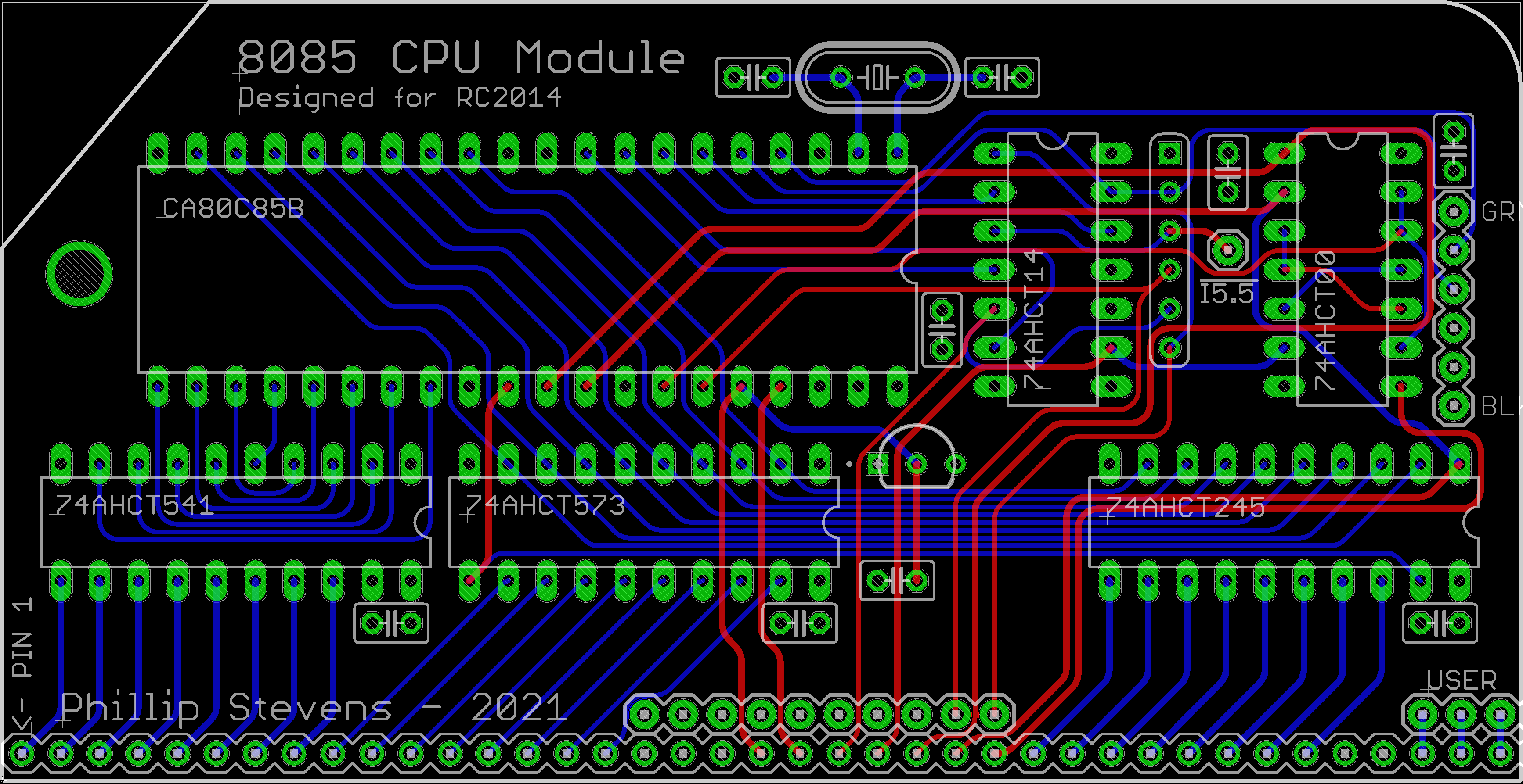
Here's a revised 8085 CPU Module and the schematic.So now only the SOD/SID serial port is on-board, and the RST5.5 is free to route to a user pin..
Let's hope the timing issues are resolved sufficiently, and it can pretend to be a Z80 well enough to fool the RC2014 standard modules.

Phillip Stevens
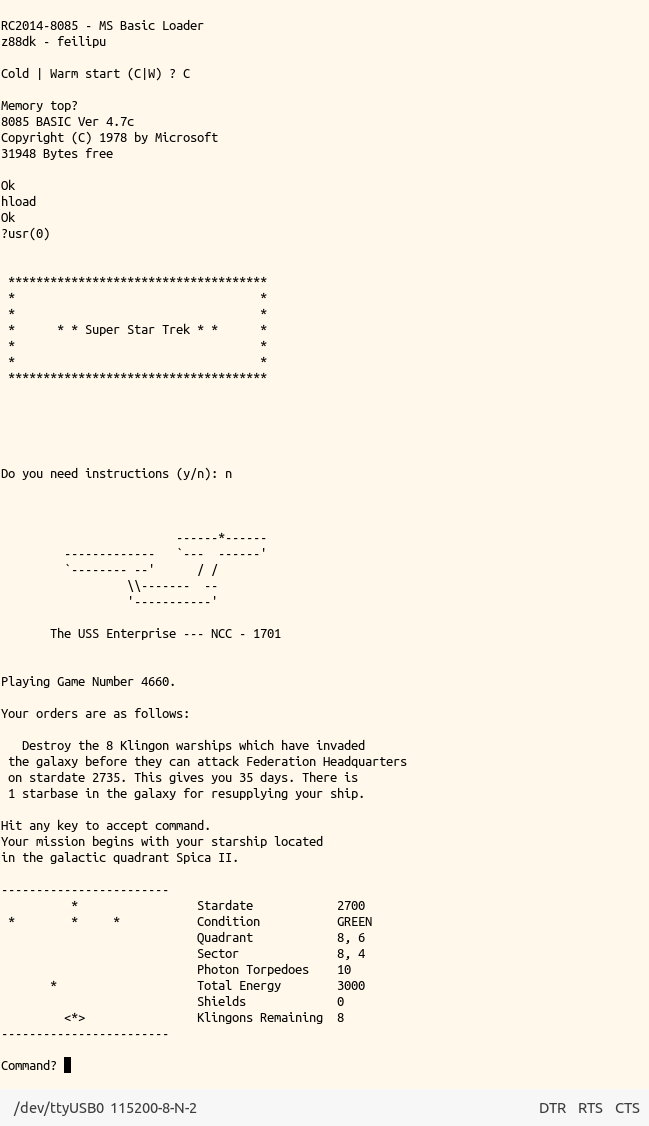
I've loaded my MICROSOFT (RC2014) BASIC 4.7C for 8085 onto a Memory Module, and the system is working fine with the standard ACIA Serial Module.I've also got the CPU SOD transmitting properly at 115200 8n2, but at this stage there's some timing issues to check on the SID receive side.
I may have to go to 38,400 baud.
The plan is to have both serial options (ACIA + SID/SOD) working jointly. With the transmission channel being selected by the most recently received byte.

Phillip Stevens
As z88dk supports 8085 C compilation using the sccz80 compiler and the classic library, whilst the RC2014 target is normally a newlib library target, there was quite a bit of interesting blending of classic and new code to get the crt0 and libraries created and linked properly. But, now the RC2014-8085 is the first 8085 platform in the newlib targets. Woo Hoo!
I've still some 8085 Module PCBs available on Tindie.
But because postage from Australia is such an expensive PITA, I've also put the 8085 CPU Module up on Seeed Fusion so anyone can order the PCB from them directly.
Chris Odorjan
I've still some PCBs available on Tindie (and have ordered some more), but because postage from Australia is such an expensive PITA, I've also put the 8085 CPU Module up on Seeed Fusion so anyone can order the PCB from them directly.
Phillip Stevens
Phillip wrote:I've still some PCBs available on Tindie (and have ordered some more), but because postage from Australia is such an expensive PITA, I've also put the 8085 CPU Module up on Seeed Fusion so anyone can order the PCB from them directly.Thanks for this, I've been meaning to ask if Gerbers were available anywhere. (Shipping to Canada from just about everywhere is bad enough, but shipping to Canada from Australia is even worse...)I see your notes on Gitlab regarding use of an Am9511A with an 8085. I've been thinking of getting the APU module for my Z80-based RC2014, do you have any plans for a revision with a wait-state generator?
Phillip Stevens
Chris wrote:I see your notes on Gitlab regarding use of an Am9511A with an 8085. I've been thinking of getting the APU module for my Z80-based RC2014, do you have any plans for a revision with a wait-state generator?Funny you should ask... See RetroChallenge 2021/10.But I can't say too much because it is not October yet, and I wouldn't want to be caught cheating.
Chris Odorjan
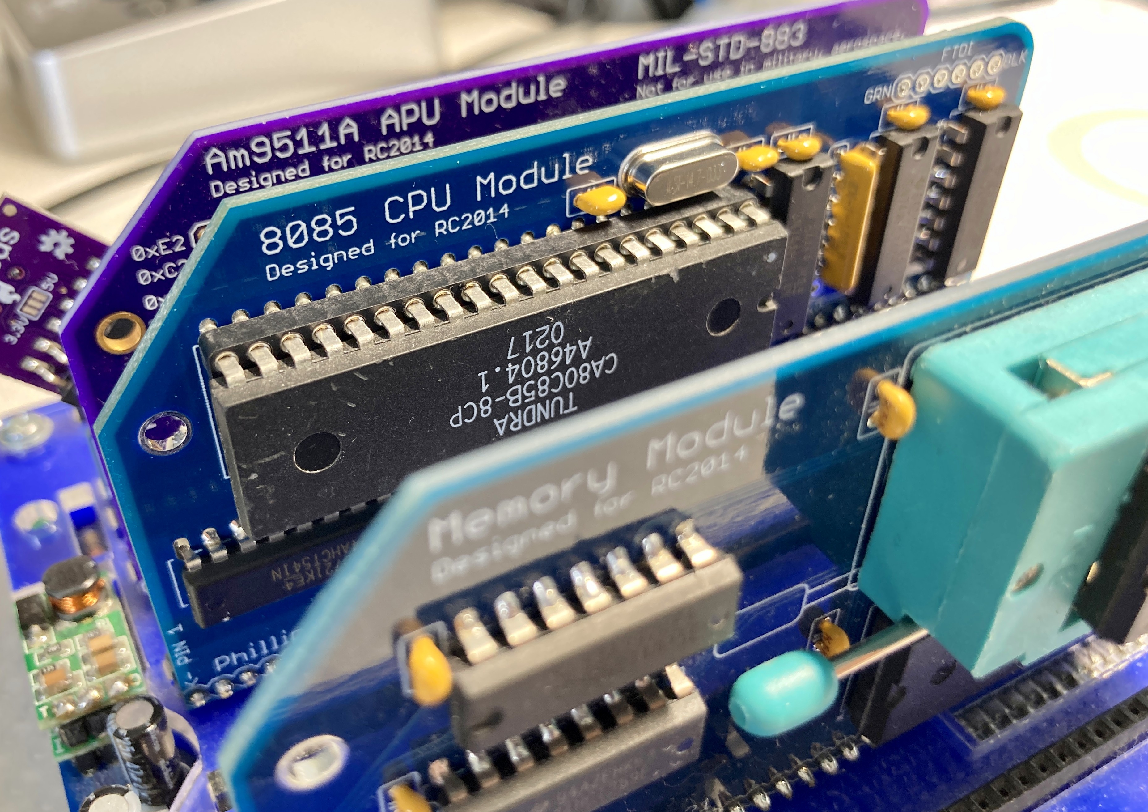
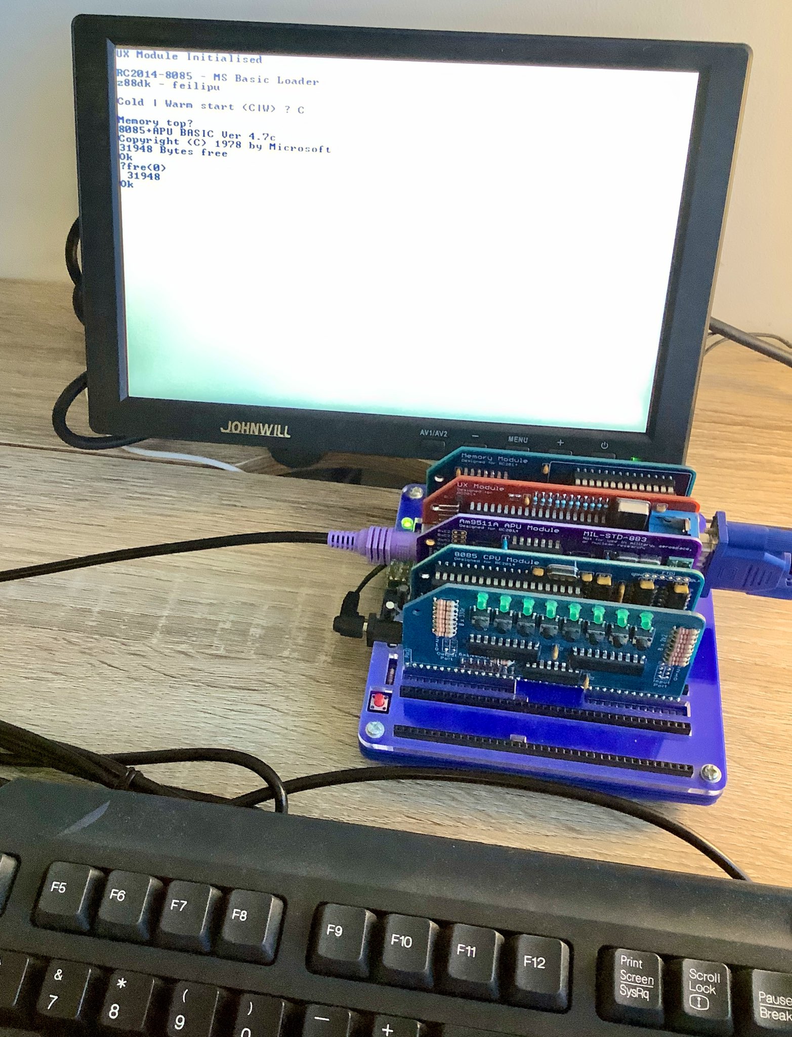
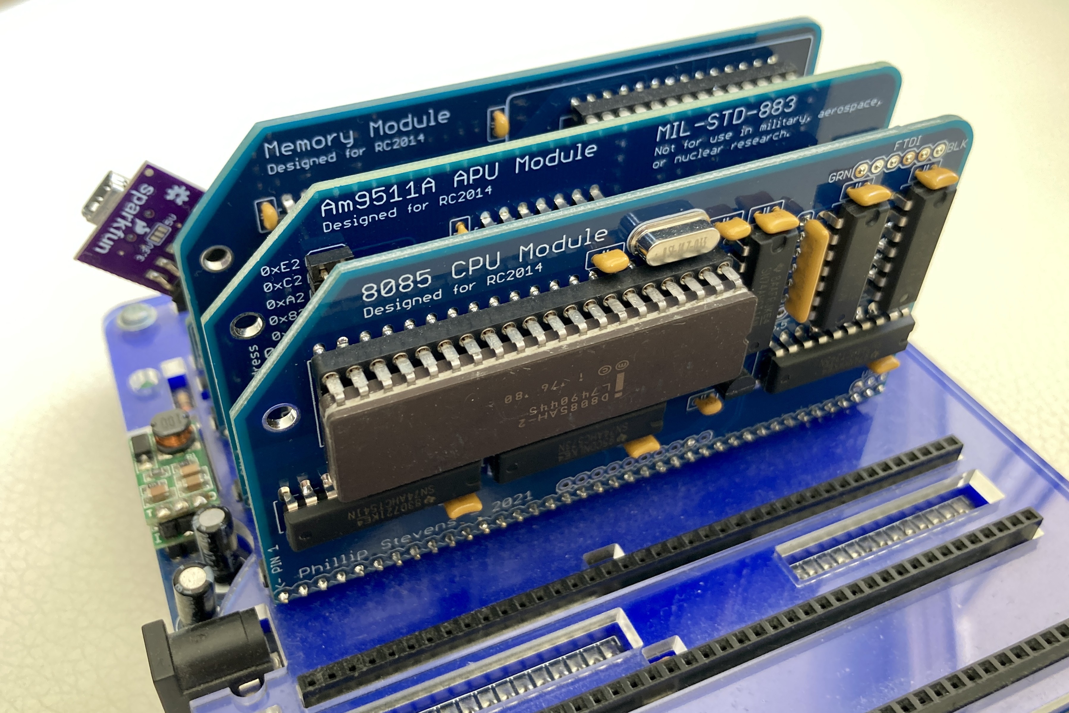
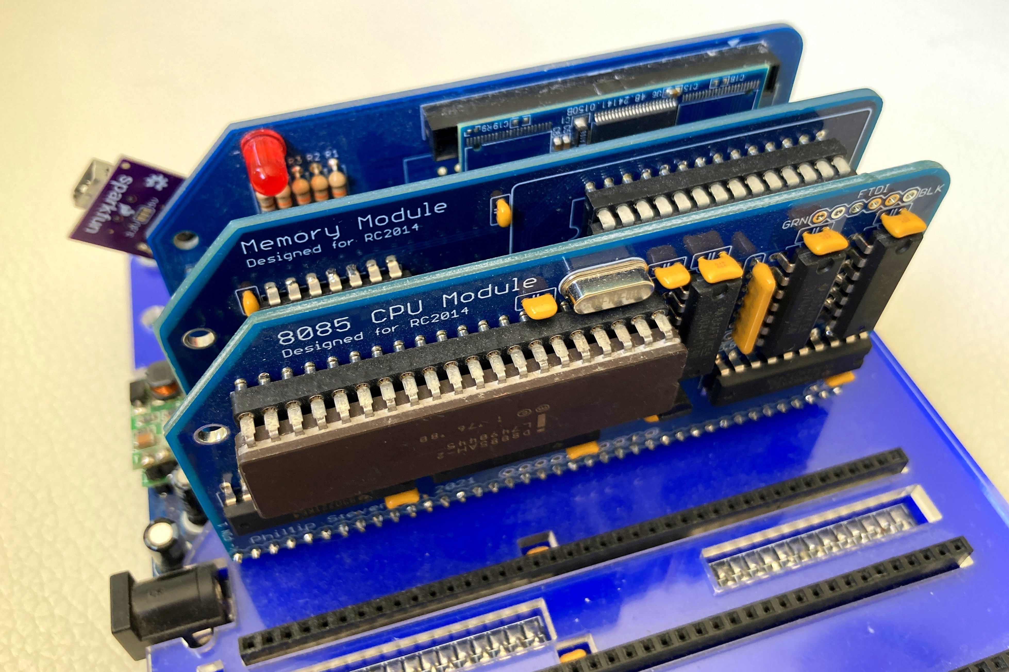
So I've been making some updates on Twitter and on my RetroChallenge Blog, so perhaps nothing here is news really. But, my new 8085 CPU Module with wait-state generator is working great with the Am9511A APU Module, and with my UX Module.There's pretty much nothing else missing that's needed, I believe.
Phillip Stevens
So I've been making some updates on Twitter and on my RetroChallenge Blog, so perhaps nothing here is news really. But, my new 8085 CPU Module with wait-state generator is working great with the Am9511A APU Module, and with my UX Module.
My currently preferred option is to run 8085+APU MS Basic 4.7c, which allows me to load compiled/assembled programs from z88dk with target +rc2014 -subtype=basic85 using the HLOAD keyword.
Since I'm effectively using the APU and 8085 together already in Basic, I've achieved the goals set for my RetroChallenge. But there a few days left. Let's see what else can be done.

tszo...@pacbell.net
Phillip Stevens
How does the Floating Point performance of the AM9511 compare to the performance of a Raspi Zero?

Doug Jackson
--
You received this message because you are subscribed to the Google Groups "RC2014-Z80" group.
To unsubscribe from this group and stop receiving emails from it, send an email to rc2014-z80+...@googlegroups.com.
To view this discussion on the web, visit https://groups.google.com/d/msgid/rc2014-z80/9f6fd32c-9e90-4b42-8090-c2d3ee56b22cn%40googlegroups.com.
Doug Jackson

Mark T
Now compare the speed of the 9511 with the z80a and similar processors of its age, to the relative speed of the rasp pi compared to an i7 or ryzen 5.
Doug Jackson
Just like an old fashioned letter, this email and any files transmitted with it should probably be treated as confidential and intended solely for your own use.
Please note that any interesting spelling is usually my own and may have been caused by fat thumbs on a tiny tiny keyboard.
Should any part of this message prove to be useful in the event of the imminent Zombie Apocalypse then the sender bears no personal, legal, or moral responsibility for any outcome resulting from its usage unless the result of said usage is the unlikely defeat of the Zombie Hordes in which case the sender takes full credit without any theoretical or actual legal liability. :-)
Be nice to your parents.
Go outside and do something awesome - Draw, paint, walk, setup a radio station, go fishing or sailing - just do something that makes you happy.
^G ^G ^G ^G ^G ^G ^G ^G- In more laid back days this line would literally sing ^G ^G ^G ^G ^G ^G ^G ^G
To view this discussion on the web, visit https://groups.google.com/d/msgid/rc2014-z80/c5901e5c-c3a3-4cad-980c-252044c7e09cn%40googlegroups.com.
Phillip Stevens
So I've been making some updates on Twitter and on my RetroChallenge Blog, so perhaps nothing here is news really.
But, my new 8085 CPU Module with wait-state generator is working great with the Am9511A APU Module, and with my UX Module.
There are some worthwhile updates for the RC2014 Classic ][, Mini, and Micro Z80 hardware (and also with APU Module) in this release too.
My next challenge is to build a native IEEE 32-bit floating point library for the 8085 and Am9511A within z88dk.
Phillip Stevens
Phillip Stevens
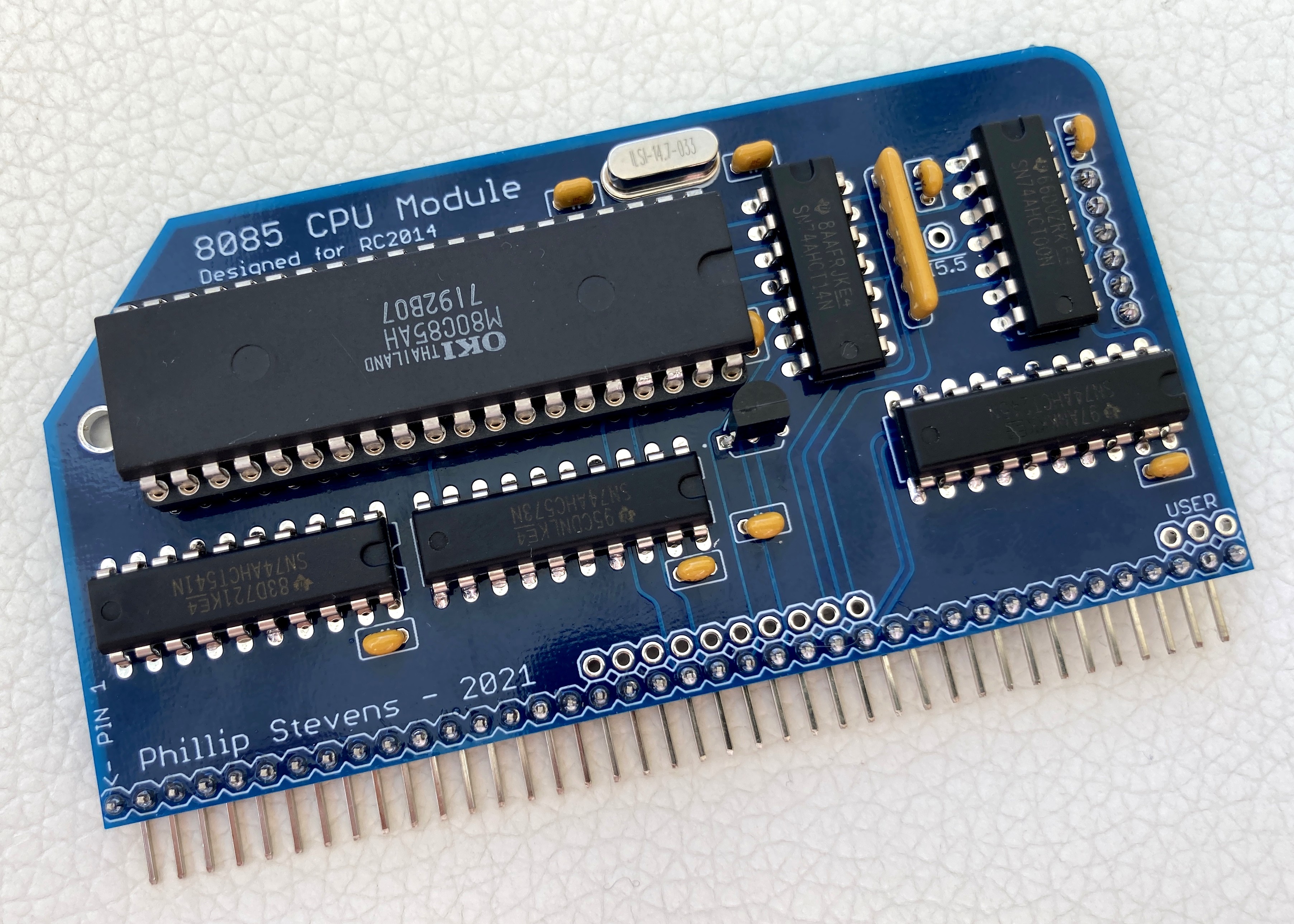
Just got some OEM pieces from my 8085 CPU Module and the 8231A APU Module. And they're working fine.Great that the older Intel HMOS 8085AH-2 part has no problem running at 7.3728MHz.And also good to have confirmed that the undocumented instructions are also there (not that there was any real doubt).
(Except the Am9511A / 8231A APU which normally runs finger ouch hot).
Phillip Stevens
I got a bit diverted into another (worthwhile) endeavour; working on the compiler support primitives for sccz80 within the z88dk.Since possibly 1998, and possibly longer, the 8080, 8085 and Gameboy Z80 CPU support has used non-reentrant primitives, with some of the code being derived from the Amsterdam Compiler Kit, which originated in the 1980s.@suborb recently went to the trouble to reorganise all of the primitives (called l_ functions), so that there is a neat inheritance process, with 8085 derived from 8080 and using common primitives. Gameboy Z80 uses its own primitives, with common primitives, and Z80 also uses its own primitives inheriting from common too. With that mechanism in place, initially it was just a process of picking functions where the 8085 undocumented instructions could contribute to better code. But, then I got a bit carried away and also rewrote all the 8080 and gbz80 primitives where necessary to ensure that the whole library was reentrant.Its been an interesting few weeks, and quite a useful end to the RetroChallenge month. Hopefully these new compiler primitives will be useful for as long as the last set were.This reentrancy will open the door to building multi-threaded systems based on the 8085. Something I'm looking forward to implementing too.And now, back to floating point...
.loop
; stuff to copy / set etc
dec bc ; 6
ld a,b ; 4
or c ; 4
jp NZ,loop ; 10
dec bc ; 6
inc b ; 4
inc c ; 4
.loop
; stuff to copy / set etc
dec c ; 4
jp NZ,loop ; 10
dec b ; 4
jp NZ,loop ; 10
Phillip Stevens
Overall, after these few months of learning about the 8085 I've got to say it feels like a much more polished object than the Z80.By that I mean the designers took something very good in the 8080 and tweaked, stretched, and polished to make it great. I like working with it, now that I've understood reasoning behind it more fully.
I'm sure everyone has their opinion, but the only thing I'd change about the 8085 would be to allow pop/push af (PSW) to be generally useful by enabling the final flag bit to store state (as is done in the Z80). That would enable another 16-bit register for stack management at the cost of just one flip-flop.
And, back to building a new floating point library for the 8085 (and trying to beat the Microsoft implementation).
- 8085+MBF32 -> 78.2 Seconds -> 12.8 kWhetstone.
- 8085+AM9511 -> 30.4 Seconds. -> 32.9 kWhetstone.
- 8085+MBF32 -> 252.3 Seconds.
- 8085+AM9511 -> 69.3 Seconds.

Todd Decker
Phillip Stevens
I'm checking the BOM of the 8085 card against my parts inventory. I have many of the needed chips in the HCT family but not in the specified AHCT family. Are they close enough that I would be okay using my stock instead of ordering new? Or, are they going to be too slow?
Mark T
Phillip Stevens
I think you might be confusing HC(T) with AC(T). AC(T) can cause problems with overshoot and undershoot when driving transmission lines, this is normally reduced by adding a series resistor to the output of AC(T).
Mark T
Todd Decker
Phillip Stevens
Thank you, Phillip. I appreciate your help and your efforts with this board. In my youth, I designed a single-board computer based around the 8085 that I never built. It will be amazing to have an 8085-based version of the RC2014 family if I can get it to work.
Todd Decker
Phillip Stevens
I've written a first draft of a "how to" and a "why it exists" for CP/M-IDE for RC2014 on my site.No coloured pictures. Quite terse, and a bit disorganised for now.But hopefully covers the points to be able to replicate the final HEX file.Todd wrote:I'd be interested in the more interesting process, Phillip. The whole reason I'm getting into the RC2014 platform is to learn things from the ground up over semi-plug and play. I have much to learn.
Phillip Stevens
Great that the older Intel HMOS 8085AH-2 part has no problem running at 7.3728MHz.
Phillip Stevens
As I'm planning to be mainly unavailable for a longish while, and so my Tindie store will be on vacation more often than not, I've published the design on Seeed Studio Fusion.The PCBs for the 8085 CPU Module can be ordered there, or the Gerberfile used to order at your favourite vendor.
Todd Decker
On Jul 2, 2022, at 9:17 AM, Phillip Stevens <phillip...@gmail.com> wrote:
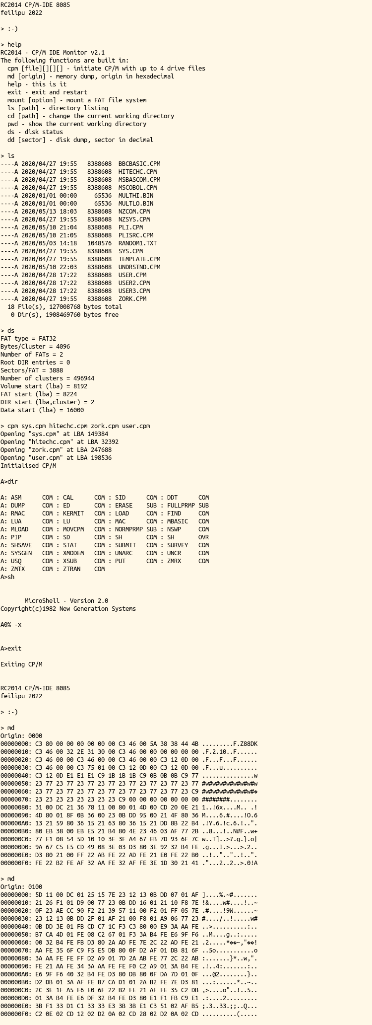
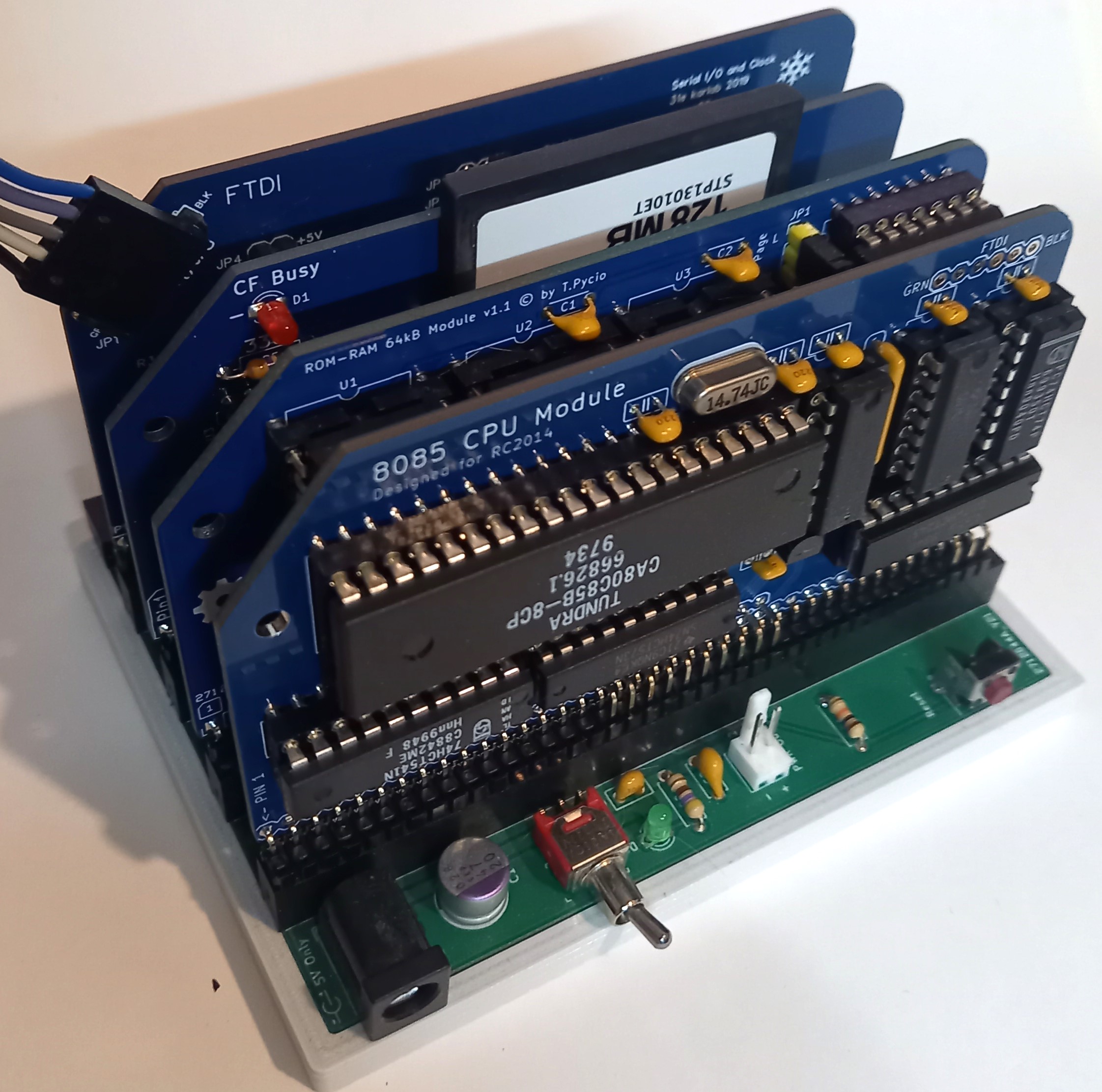
Phillip Stevens wrote:As I'm planning to be mainly unavailable for a longish while, and so my Tindie store will be on vacation more often than not, I've published the design on Seeed Studio Fusion.The PCBs for the 8085 CPU Module can be ordered there, or the Gerberfile used to order at your favourite vendor.Just noted that Spencer has finally obtained the unobtainable 82c55 devices for his IDE Hard Drive Module and has them for sale on Tindie and z80kits.I guess even a 78 week lead time comes to an end, eventually.I mention that because I've only 6 remaining 8085 CPU Module PCBs left on Tindie, and 8085 CP/M-IDE needs the IDE Hard Drive Module.So if you're interested in having an 8085 CP/M computer, compatible with the RC2014 bus, then this is the chance.This shows the 4 Module CP/M-IDE, with ACIA Module, IDE Hard Drive Module, Memory Module, and 8085 CPU Module.
<IMG_1688.jpeg>Once these 6 are gone, then the next option will be either the Gerbers (or PCB order) from Seeed Studio as noted above.For reference, this is how it looks on the terminal.
<cpm-idev6.png>Cheers, Phillip--
You received this message because you are subscribed to a topic in the Google Groups "RC2014-Z80" group.
To unsubscribe from this topic, visit https://groups.google.com/d/topic/rc2014-z80/qo7nfDZmY-k/unsubscribe.
To unsubscribe from this group and all its topics, send an email to rc2014-z80+...@googlegroups.com.
To view this discussion on the web, visit https://groups.google.com/d/msgid/rc2014-z80/9d5ae64e-a910-494a-95d6-db1b566b1249n%40googlegroups.com.
<cpm-idev6.png><IMG_1688.jpeg>

Spencer Owen
Phillip Stevens
Added a few more sections on the end of CP/M-IDE for RC2014.I think that covers most of the things needed to understand how a C shell is useful for CP/M, and where all the pieces of code come from, and why they're used.
Todd wrote:I'd be interested in the more interesting process, Phillip. The whole reason I'm getting into the RC2014 platform is to learn things from the ground up over semi-plug and play. I have much to learn.
Phillip Stevens
Alan Cox
instructions they got used. Even the Small C for 8085 uses them.
> Specifically the 8085 acia version of CP/M-IDE is more than 1,500 bytes smaller than the z80 version (28178 bytes versus 29767 bytes). This saving comes mainly from the FAT file system library, where access into structures is very common. The CCP/BDOS/BIOS code is essentially the same as the original DRI 8080 code, and doesn't contribute much to the relative savings.
compact code than the Z80 one, and usually faster. That's without
having taught it how to use the spare BC register pair as register
variables.
Alan
Phillip Stevens
Alan Cox
Where did you get the ANSI 8085 C compiler? Is it public domain?I'm planning to do some more 8085 benchmarking over the coming weeks, so I'd love to add it into this numbers game.
Phillip Stevens
Tadeusz Pycio
I guess I'll have to design your module, as the Gerber files won't accept JLC, and buying on Tindie is out - shipping is a couple of new designs from the PCB factory :( I will look into this at my leisure.
Phillip Stevens
Bill Shen
Bill

Dave White
Alan Cox
>
> I'd be interested in making one too. I have four 8085 chips sitting here looking for a use. I'd also be using JLCPCB for boards, so if you could make Gerbers compatible with them, that would help a few of us out.
are in the UK I may have a spare or two left for postage cost.
https://hackaday.io/project/167859-80c85-and-mmu-for-rc2014-bp80
Currently running mine with an 8MHz Tundra 80C85.
Alan
Dave White
Tadeusz Pycio
Phillip Stevens
I'd be interested in making one too. I have four 8085 chips sitting here looking for a use. I'd also be using JLCPCB for boards, so if you could make Gerbers compatible with them, that would help a few of us out.
Dave White
Bill Shen
Bill
Dave White
Phillip Stevens
Tadeusz Pycio
Tadeusz Pycio
Phillip Stevens
As I'm planning to be mainly unavailable for a longish while, and so my Tindie store will be on vacation more often than not, I've published the design on Seeed Studio Fusion. The PCBs for the 8085 CPU Module can be ordered there, or the Gerberfile used to order at your favourite vendor.
Great that the older Intel HMOS 8085AH-2 part has no problem running at 7.3728MHz.I also got an 8231A Intel branded APU, which also works fine in the APU Module.I'm very happy to have a fully CDIP Intel RC2014 system.

Phillip Stevens
On Saturday 7 May 2022, Phillip Stevens wrote:As I'm planning to be mainly unavailable for a longish while, and so my Tindie store will be on vacation more often than not, I've published the design on Seeed Studio Fusion. The PCBs for the 8085 CPU Module can be ordered there, or the Gerberfile used to order at your favourite vendor.Great that the older Intel HMOS 8085AH-2 part has no problem running at 7.3728MHz.I also got an 8231A Intel branded APU, which also works fine in the APU Module.I'm very happy to have a fully CDIP Intel RC2014 system.

 8085 CPUs Tested
Some very simple testing was done to determine how much current each CPU implementation required, and from this it is clear which devices are implemented in NMOS, and which in CMOS.
Phillip Stevens
ld de,hl+2
ld hl,(de) ;l_gint
push hl
call regexec
call l_gint2
push hl
call regexec
ld hl,8
add hl,sp
ld a,(hl)
inc hl
ld h,(hl)
ld l,a
ret
inc hl
inc hl
l_gint:
ld a,(hl)
inc hl
ld h,(hl)
ld l,a
ret
regex 1968512 2276653 2242505 1925245 14%
Alan Cox
How useful could it be to have a special case for certain comparison operators? Well a quick look at the ChaN FatFS code shows more than 500 equality operations, and 300 inequality operations. Similarly the z88dk regex library function has many equality and inequality operations included.So I recently included special cases of equality and inequality comparisons using sub hl,bc into the z88dk 8085 library support.The improved 8085 equality operation looks like this, compared to the original 8080 compatible version here.
Phillip Stevens
So I recently included special cases of equality and inequality comparisons using sub hl,bc into the z88dk 8085 library support.The improved 8085 equality operation looks like this, compared to the original 8080 compatible version here.
Interesting. I considered something similar on the Fuzix compiler for 8085 mode but as I use BC as a register variable it was a bit too convoluted and register variables seemed more valuable, particularly as the compiler is smart enough in most cases to know when only flags are needed (so can do mov a,h ora l).
There are other places it using BC seems to help - some maths ops seem to work out nicer with DSUB that way so I do wonder if someone in Intel there were reference implementations of div, mul etc tuned for the new instructions.
For me this is part of the fun of playing with z80/8080. It is still possible to make things better with simple code tweaks, even 50 years later. I can see the resulting assembly get better "prettier", and my C program executable getting smaller and faster.
Phillip Stevens
But recently I've been wondering about the sub hl,bc instruction. Why was it so important to have a subtraction instruction when two complement numbers can be subtracted easily using the addition instruction? Why id sub hl,bc win its place in the limited opcode space?Well it turns out (I believe anyway) that the 16 bit subtraction instruction sub hl,bc is really intended for efficient comparison operations. In C it is quite common to end loops with equality ( == ) or inequality ( != ) operators, and these can be quickly implemented with the sub hl,bc instruction. Subtracting two numbers quickly generates a signal (zero flag) to either equality or inequality depending on what you want to test.How useful could it be to have a special case for certain comparison operators? Well a quick look at the ChaN FatFS code shows more than 500 equality operations, and 300 inequality operations. Similarly the z88dk regex library function has many equality and inequality operations included.So I recently included special cases of equality and inequality comparisons using sub hl,bc into the z88dk 8085 library support.The improved 8085 equality operation looks like this, compared to the original 8080 compatible version here.And as a result the regex library function test is now faster on 8085 than it is on z80!So yes, definitely worth doing.Test Z80 8080 8085 Yesterday 8085 Today Improvement
regex 1968512 2276653 2242505 1925245 14%

7alken
(reported to z88dk github and fixed next day!! ... while my own code is on hold for 2yrs) found by VMEX tests here:
... Z88DK compiler for Z80 fails with "unsigned >" comparison (BGTU)
https://github.com/apws/230326-VMEX
I am all the time considering also some RV32EM isa extensions in VMEX (as it is binary different already) to make it more "human face" for asm coding,
making notes here and already some changes to encodings ... its slowly evolving, as I am now mostly focused (I last month in turbo mode)
CPLD "northbridge" links to memory only and "southbridge" only down to base-board and decoupled peripherals over 7xbus (MIPI 16bit + SPI)
P.
PS: I myself defined retro for me as anything parallel before fast serial/differential madness ))
Alan Cox
Over the past weeks I've been thinking further about the use of sub hl,bc for comparison operations.In particular combined with the jp k,nnnn and jp nk,nnnn instructions added to the 8085 instruction set.Kevin Shirriff provides a very detailed view of the implementation and use of the 8085 specific K flag, and its use in signed comparisons.

Mats Gülich
I remember computer magazines were filled with articles about CP/M for instance as an operative system which was a new invention. One could run a program based on other programming code than mnemonics or machine code.
The retro trip is also for me back to basics about to handle the possibilities in a given hardware and building my own hardware, as we did back then, in the "good old days". 😎
//Mats G.
--
You received this message because you are subscribed to the Google Groups "RC2014-Z80" group.
To unsubscribe from this group and stop receiving emails from it, send an email to rc2014-z80+...@googlegroups.com.
To view this discussion, visit https://groups.google.com/d/msgid/rc2014-z80/CAK9X0%2BvwCjgmfcCtCZomDa80nZ4bi6Lwmersa%3DEQmyMp6K_HJw%40mail.gmail.com.
Phillip Stevens
Over the past weeks I've been thinking further about the use of sub hl,bc for comparison operations.In particular combined with the jp k,nnnn and jp nk,nnnn instructions added to the 8085 instruction set.Kevin Shirriff provides a very detailed view of the implementation and use of the 8085 specific K flag, and its use in signed comparisons.
For constant equality however you can also use addition so you can also use de and that works on 8080 by just negating the constant and doing a dad (add hl, in Z80 speak).
The 8085 additions were very well thought out whereas the Z80 appears to have been a bit of a "whee how many things can we add" exercise in places.