Z80-PC mainboard - progress update - PCBs ordered

1,222 views
Skip to first unread message

Rodney Knaap

unread,
Jan 14, 2022, 8:55:56 PM1/14/22
to RC2014-Z80
Hello everyone,

It has been a while since I last posted here, I have worked hard on my project!
I have no idea if anyone is interested, but my project is still in the beginning stages now!

I have completed the mainboard PCB design and ordered some PCBs from a Chinese PCB factory. I have added a screenshot of the KiCad 3D viewer so you can get an idea of the board. It's 12 x 8,35 inch in size, and fits an ATX case, the slots should all match up properly.

The mainboard contains the following functionality:
- Z80 CPU
- ROMWBW compatible bankswitching with 7 memory chips, 3,5Mb, first bank is flash ROM, then RAMs, memory 6 can be jumpered to be RAM or flash ROM
- PPIDE interface
- RCWDC floppy drive interface
- serial ACIA with USB to UART connection onboard for interfacing with a normal PC via USB cable
- TMS9918 graphics with composite output (I still need to verify color output, I have a PAL TV, and maybe the clock needs to be changed as well)
- dual YM2149 sound, IO ports connected to pinheaders
- dual SN 76489 sound
- potmeter adjustable sound mixing onboard for left and right channel mixed output of YM and 76489 sound to each channel
- cassette tape interface via 2 bits of a transceiver and some simple filtering circuits, somewhat similar to a ZX81 or spectrum. another nice retro programming project!
- VT82C42 PS/2 keyboard and mouse controller
- DS1302 realtime clock
- RTL8019AS Ethernet interface (on plug-in mini PCB with only the SMD chip, rest is onboard through-hole components)
- ATX power supply control via pushbutton, and software controlled power off circuit.
- timing clock-based (not R/C timing!) power-on reset circuit with sufficient hold timing to allow the ATX PSU to stabilize. (my own circuit verified and tested, long story!)
- LED outputs for signalling system controls including driving transistors for the LEDs. Total something like 18 LEDs including for ethernet link, RX and TX. I will make a separate frontpanel LED board which plugs into the mainboard via 3 small headers.
- 8th memory chip on a separate PCB merged with a custom GPU controller

The custom GPU controller with VGA output passthrough on the mainboard is planned to be the next project after testing and verifying the mainboard. The GPU board will use a raspberry pi zero and bare metal programming as mentioned before. I plan to test first with handshaking protocol between Z80 CPU and raspberry pi using asynchronous bus switching to 512 kb of shared RAM to exchange graphics data and commands from the Z80 CPU. I plan to try handshaking via a control/status port method which will be used to switch the bus to the shared RAM. Shared RAM will be an exchange system to transfer screen data and screen commands from the Z80 into the memory of the GPU which will then execute the commands as provided. That's the plan so far, I will see how it performs when I get some basic functionality programmed. This will be quite a project to program these functions. I will use no OS on the raspberry pi, only using the CPU and programming it to function as a custom graphics controller. At least, I will try if this can be achieved with the raspberry pi zero. At least it has enough processing power and memory.

I have split the Z80 bus into a memory and IO bus, also to devide the TTL loads. Basically everything goes through bus transceivers, which I still need to verify to work as intended.
The IO bus goes to the onboard IO interfaces and there is a separately buffered expansion bus which goes to 6 reduced pin expansion card edge slots, only for I/O. I have added some termination on the expansion slots in case it's needed.
Also I have made the /INT input of the Z80 into a "party line" for any IO expansions which need interrupts. I will of course have to look into the software side of things how to answer the calls!
Current members will be the ACIA, TMS graphics and the realtek ethernet controller. I added a WAIT circuit for the Z80 as described by the realtek datasheet.

There is a CPU connector for future upgrades or replacement of the CPU. Perhaps with an FPGA core in the future.

The GPU card will plug into the memory bus and IO databus for exchanging data and commands.

Of course, ethernet and mouse control, that is all without software, I just followed the manufacturer datasheets for interfacing to get the hardware side built first.

So now I am waiting for the mainboard PCBs to arrive so I can build one and test everything!

I'm looking forward to find out if the mainboard bus timings will work through the transceivers as intended, and to get started with the raspberry pi zero in bare metal programming!
I am prepared for much further troubleshooting to get the transceivers working! Unfortunately I don't own a fast oscilloscope yet! I decided to just build up the mainboard and test on that, rather than to build more testing PCBs using point to point wire soldering! Since the system is growing, I really need something solid to test and develop further on! So I may be rewiring some things in case of any problems.

To build a Z80 PC has been an idea of mine for a long time!
To use it as a programming and development platform for me is the best excuse to finally try to do it and get even more use out of the PC!

Ideally I would love to also try porting applications to the Z80 from other systems such as the IBM compatible PC!
And I am planning to create some games on the system, and control those with a SNES controller, another small hardware addition which I am planning.

I will post back here as soon as I have some further progress made on the system.

Mainboard.png
That's all for now, I should change my website as well soon!

Kind regards,

Rodney

kurt....@web.de

unread,
Jan 15, 2022, 4:28:58 AM1/15/22
to RC2014-Z80

Hello Rodney,

I like it. A great product.
I wish you every success.

Greetings from Germany
Kurt

karlab

unread,
Jan 15, 2022, 6:32:46 AM1/15/22
to RC2014-Z80
It looks great.
Have you considered using the Z180, it would simplify the design?
Karl

Rodney Knaap

unread,
Jan 15, 2022, 10:08:50 AM1/15/22
to RC2014-Z80
Hi Kurt,

Thanks for your message and kind wishes!

I am glad to finish the design stage which took a long time to complete.

Making a simple circuit for controlling the ATX power up and reset has proved challenging when I started to test things. It proved really funny how circuits can behave when parts are in a powered off state, connected with the standby circuits which are powered all the time. Especially CMOS ICs have a strange behaviour which lets them draw power from input pins and not entirely be powered off! I used a 4020 counter which simply didn't reset after powering off! (or rather, not powering off!) That is really tricky and I haven't observed such a behaviour from ICs before! haha! I heard Bil Herd who worked at Commodore before mentioning about this fenomenon recently on youtube, unfortunately too late for me to learn about this because I already discovered it myself, a lesson I won't forget! I know I could have programmed some small controller like an ATMega or even smaller for this purpose, but I still like this method more for now, even if it uses a few chips.

I hope that the I/O timing will be fast enough for everything.
Or else I may have to revise the IO decoder circuits entirely.
I made some standardised decoding circuits which can wire up any I/O address as needed.

Karl, thanks for your message!
Definately the Z180 has been in the back of my mind.
For me, this process is fluent and may change along the way.
Making this PCB has been a natural next step in my process to connect things that I want together in a solid way, and the plan may change later.

I wanted to get away from those initial hand wired PCBs which after joining 6 PCBs showed me the potential of a very complete Z80 system, enough so that I committed to this mainboard PCB stage with enough circuits to fill it, rather than designing and building more separate interface PCBs, which would also consume a lot of time.

I ordered some Z84C0020 DIP ICs from Aliexpress, and found them to be relabeled old CPUs, some of which thankfully qualified to run at 7,3728 Mhz. I do want to test at 20Mhz later on the mainboard, so I will be looking for other suppliers. Indeed, using a Z180 may be an easier step to get up to 20Mhz, I will look into that too. I need to take some time to study the documentation and examples of the Z180.

Also I am realising that my system still doesn't have a timer included, which may prove necessary later for software which require some stable and regular flow.
I can build some changes up on expansion cards, and later move them onto the mainboard in next revisions.

I am still looking at adding an FPGA for the GPU card right now, especially after seeing the MiSTer FPGA project, and the comments on that website do make sense, notably that FPGAs can do certain things better and faster than processors which are more sequential in nature. Definately a hybrid design similar to the MiSTer would be even more capable and desirable, however surely also more complex to master. I just need to get more experience in this field, to lower the threshold for possibly getting into this kind of setup.

Naturally, I know that what I am doing is rather inefficient design. Many circuits could be integrated into a small number of chips, or even using chipset ICs. Anyway, for now the focus of my project is not to be efficient, but to first get a transparent system running, and to have a suitable platform which can benefit from some coding work. It's also a process of getting more experience for me, for which a system made like this is much more suitable. When I look at my old projects from the late 90s, this is entirely another level, so I want to progress in this line forward, and get more experience in assembly coding, and maybe in other languages. I want to get more hands-on experience in hardware development as well.

I just seem to love the idea that I can take an ISA card from my AT 286 PC, and take that floppy controller chip, put it into the socket on my own mainboard, and it works! It does have a lot of charm for me!
Recently I am getting a new and much broader perspective on early IBM compatible PCs and that evolution as well, which is also a new appreciation for them!

I will update here later, the PCB factory is already making the PCBs at the moment, they are really lightning fast and already working on the solder mask.

Kind regards,

Rodney

PCB image.png

Op zaterdag 15 januari 2022 om 12:32:46 UTC+1 schreef karlab:

Patrick Jackson

unread,
Jan 15, 2022, 4:03:40 PM1/15/22
to RC2014-Z80
I will be watching this project with great interest, will definitely consider buying one if possible!

Mircea Teletin

unread,
Jan 16, 2022, 7:45:16 AM1/16/22
to rc201...@googlegroups.com
Hey Rodney!

Simply put: I want one! :D

Mircea

--
You received this message because you are subscribed to the Google Groups "RC2014-Z80" group.
To unsubscribe from this group and stop receiving emails from it, send an email to rc2014-z80+...@googlegroups.com.
To view this discussion on the web, visit https://groups.google.com/d/msgid/rc2014-z80/2f9ccb76-f477-41f5-8bb8-3896d36e036fn%40googlegroups.com.

karlab

unread,
Jan 16, 2022, 8:56:06 AM1/16/22
to RC2014-Z80
Hi Rodney
If you are looking for obsolete chips, I would recommend Utsource.net.
Needless to say, I want one when the product is finished.
Karl

On Saturday, 15 January 2022 at 02:55:56 UTC+1 rodne...@gmail.com wrote:

Rodney Knaap

unread,
Jan 16, 2022, 11:10:36 AM1/16/22
to RC2014-Z80
Hi Karl,

Thanks for the suggestion, I remember buying some old chips from Utsource years ago.
I think some old floppy controller chips for the ZX81.
I will have a look at their website.

I am doing this work purely for the hobby and love of retro computing!
I am always looking to gain more development experience, and definately willing to openly share this work with anyone who is interested!
Hopefully I can help to elevate the Z80 platform further in the same spirit as what I found before!

Karl, it was great to see your designs and ideas, they also helped to inspire me for making this mainboard!
Also, Wayne Warthen's super valuable software work to give us ROMWBW was also most essential to be able to test and confirm the circuits and the whole system!

I will post my test results here as soon as I receive the PCBs!
Anyone who likes my project can check back here.
Also when I have the chance to update my website, I will post a message here.

Right now while I am waiting for the PCBs I am gathering information about the raspberry pi zero to get some direction in my prototype GPU PCB.
That will be next!

Also I will design a small adapter PCB for the realtek ethernet SMD chip to plug into the mainboard, I will combine that with the GPU PCB order.
I already sorted out all the jumper mode configurations for that from the datasheet.

Thanks for your interest everyone!

Kind regards,

Rodney

Op zondag 16 januari 2022 om 14:56:06 UTC+1 schreef karlab:

Rodney Knaap

unread,
Feb 13, 2022, 9:02:49 AM2/13/22
to RC2014-Z80
For anyone who is interested or curious about my Z80-PC project, I have many things to report:

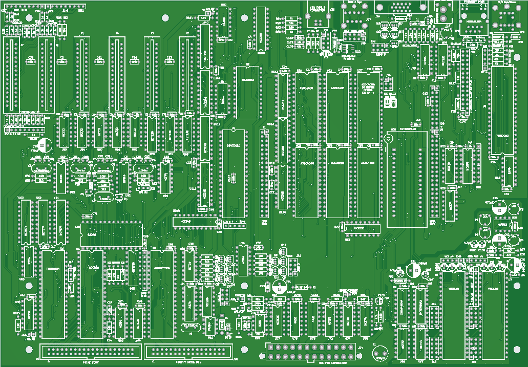
I have received the manufactured mainboard PCBs from JLCPCB (a big recommendation from me!) and built one up. At first I have connected all the ICs which were necessary for basic function and starting via ROMWBW HBIOS software.

During my test work I have found some issues, as I expected. I was not able to test several things on my previous hand wired setup because I would have to dramatically alter all the PCBs in such a way that it would have been much more work than manufacturing and building up this mainboard, and would have been considerably less stable and solid.

The issues I have found were:

  • I need to rename some signals in the ROMWBW bankswitching circuits because I used the naming convention "MAxx" for all the address lines which control the memory ICs after separating the memory and IO bus. Specifically the A14 and A15 lines need to be taken from the Z80 directly to the bankswitching register ICs, which then control the memory IC MA14 and MA15 lines amongst others. I have disconnected those pins on the registers with an extra socket inbetween, and taken the signals from the CPU directly to the registers with a few wires.
  • There is an I/O timing issue (of course!) with the decoder which creates the IO direction signal for the I/O data buffer. Apparently one extra gate in the signal path from /IORQ is creating a delay which is too long to get the data on the bus fast enough for the CPU to handle it. I have taken out the /IORQ and /M1 evaluation gate for the time being, since it is only necessary for certain /INTACK events which are currently not used. I will see how I can solve the problem to later include /M1 for the /INTACK conditions.
  • I wrongly assumed that for ROMWBW IO ports the not decoded A3 line should probably be low, however this turns out to break ROMWBW function. I temporarily disabled evaluation of the A3 line and simply wired it true. After this I found that ROMWBW initialized properly.
  • my ACIA was not working, I needed to change the IO port in the ROM.
  • I will change the mounting holes of the mainboard to include some grounding pads and vias inside them as we see on brand manufactured mainboards. This is simply a small change to make the mainboard more solidly grounded to the chassis, which is not an actual issue but simply better to do so.
  • I need to move one IC down a millimeter or two to create more spacing for the IC packages to fit more easily.
  • I need to change the clock crystal footprint because apparantly the 32768 Hz crystals do not come in HC49S packaging. Probably I will switch to a tube shaped crystal.
  • I need to change the RESET (positive logic) line because using it in this way creates problems in my power up and reset circuits. I probably need to invert /RESET another time with an inverter and route that signal to the PPI and FDC. For the time being I separated the RESET pins from the PCB with an extra socket and wired the RESET lines manually with a resistor to ground. So far I didn't find any problems with the PPIDE or FDC even without a reset occurring on them.
  • I will see about possibly adding a trimmer capacitor to the clock generator for the TMS. This may help in the future to slightly adjust the clock for better display.
  • I will be adding some pull up resistor packs to the databus and maybe also to the address bus in several areas. This will help to improve the signal stability and reduce reflections as well. I really need to get a suitable oscilloscope to evaluate all the signals for stability and see if there are any issues that can be otherwise improved. I do have a HM205-3 scope but I am currently repairing a broken off control where I need to replace a shaft on one of the potmeters. After that I can test this scope and see if it can be sufficiently accurate at this frequency to look at the bus signals and see how I can make some improvements from actually seeing the signals. Later when I get a 20Mhz Z80 I will test and look more at the signals for that frequency.
  • The SN76489 sound generators are quite noisy. I will think about some method to disable them when they are not in use, or to initialize them at boot of the PC to become more "quiet".
  • the I/O databus is currently not working with a 74HCT245 transceiver, I am using a 74LS245 for the time being, after getting my scope operational I will do further testing to find the issue with the 74HCT245.
  • the LED pins on the ethernet connector are slightly off, but still able to assemble it onto the PCB correctly. I will adjust the LED pins a little on the next PCB revision.

Basically, that was it so far up until this point. Only a few small changes were needed to get things running on the mainboard PCB. I am very happy that the big change of using the bus transceivers didn't experience too many difficult problems. It was to be assumed that because it alters the timing that some issues might occur since I was not able to test anything before yet, but I am pleased to be able to separate the bus and buffer everything successfully according to plan. Also the I/O address decoders which I totally changed to a more standardized design were all working properly.

I was able to test one of the YM2149 sound chips which operates on the MSX standard ports, which works with the TUNE.COM CP/M program. It is working fine which confirms my YM port circuits to be correct. That also means that the second YM2149 chip will work fine with software that can support it.

I am waiting for some components to arrive from China, which is of course rather delayed because most people in China were celebrating the spring festival with their family. So I will do further soldering and testing as soon as further parts arrive. I desoldered some things from a few PC mainboards so I could at least test things sooner.

So what I have confirmed to function is:

  • ROMWBW
  • PPIDE
  • RCWDC floppy controller
  • ACIA
  • YM sound on one chip, I need to see if any software is available to test both YMs for a total of 6 channels
  • DS1302 realtime clock
  • ATX power supply control
  • power-on reset circuits
  • PS/2 keyboard interface

After receiving further parts I will be testing:

  • TMS video output
  • USB direct cable connection to PC for ACIA serial output
  • mixed audio output to speakers

After getting the last things tested and getting all the bus signals optimized, I will move on to have the PCBs made for the RTL8019AS ethernet chip to plug into the mainboard. After that I will probably move on to the GPU design.

Possibly I will design a second revision mainboard right away, just to get rid of the wired fixes and have a 100% signal optimized system which needs no modifications as a solid basis to continue.

Further updates will follow below on this thread!

Img_8915s.jpg
Op zondag 16 januari 2022 om 17:10:36 UTC+1 schreef Rodney Knaap:

Mircea Teletin

unread,
Feb 14, 2022, 2:37:21 AM2/14/22
to rc201...@googlegroups.com
Boy do I want one now :-)
Let us know how may we help!

Best regards!
Mircea

--
You received this message because you are subscribed to the Google Groups "RC2014-Z80" group.
To unsubscribe from this group and stop receiving emails from it, send an email to rc2014-z80+...@googlegroups.com.

Doug Jackson

unread,
Feb 14, 2022, 3:03:26 AM2/14/22
to rc201...@googlegroups.com
Hi Rodney,

That is a beautiful board - I would be very interested in the next version as you progress the design.

May I please offer a small thought from working with electronics for my entire life -  Your board is beautifully designed, but the only issue I see is that you should work really hard at always making the orientation for all of your IC's consistent - i.e. all vertical IC's pin one top left, and all horizontal IC's pin one bottom left - or top right.

It greatly simplifies assembly as well as faultfinding later.

Also, it may be worth reconsidering the 5 separate crystals - are there common frequencies? 

I really appreciate your comment about dealing with standby voltages - CMOS is painful in its ability to merrily power itself using voltage through input pins.

Kindest regards,

Doug Jackson

ph: 0414 986878

Check out my awesome clocks at www.dougswordclocks.com
Follow my amateur radio adventures at vk1zdj.net


--

Gary S

unread,
Feb 14, 2022, 6:35:02 AM2/14/22
to RC2014-Z80
I actually quite like the idea of this board..

BUT, it actually has been bugging me for a little while...
today it finally clicked...  "PICMG 1.0"

For a number of years when moving to rackmount for my ISP we went to "PICMG 1.0" as an experiment so that we actually had an easy & relatively cheap upgrade path in the then changing processor market.

So I wonder would it be cheaper an easier to have a z80 SBC which utilises that system ? 

Gary
vk2zbb

Patrick Jackson

unread,
Feb 14, 2022, 11:21:45 AM2/14/22
to RC2014-Z80
Looks absolutely AWESOME. I'd LOVE to get my hands on one of these boards once you deem them ready!

Rodney Knaap

unread,
Feb 15, 2022, 11:17:56 AM2/15/22
to RC2014-Z80
Thanks everyone for your replies! I much appreciate to hear from you, nice to see some interest!

About the crystals, you are right! I have also been thinking about possibly using another method for generating clocks,. Maybe using a single crystal and deriving clocks from that somehow would be cool, I think there should be various methods for that. And of course that would be an interesting thing to do, especially  if it could be done with standard ICs. It also depends on how much time it would take, I may look into that. Also, I remember that the TMS outputs a CPU clock which could be used. My only concern on doing that was the quality of the clocks on the TMS output which is unknown to me. I do put signal integrity and stability far above component count for example. I could check the TMS output. On the other hand, maybe not everyone may want a TMS! :)

Anyway, all the points I am reading all make sense and are valid things and I will keep them all in mind, thanks!

As far as form factor is concerned, from the cost perspective I am not planning to change it at the moment. A single PCB cost me around 10 euro including the shipping costs from JLCPCB, to my great surprise! So I am not really looking at saving on the PCB costs. I may even increase the size a little because the mounting holes on the bottom are not a standard location, which would need some holes to be drilled in the case for those mounting points. Of course, also not a really big issue either. It is really a different time today, and things have improved a lot on the PCB factory side of things, thanks to Chinese industry!

I hope I can get my scope fixed soon, and that it will be helpful to improve quality of the bus signals. That will be definately something I will be looking at in much detail! The most important thing I want is completeness of the system and gaining as much stability as possible. 

After getting this system in a state that I feel it's not needed to change anything anymore, a next step may still be to design the system in other forms, if that would have some appeal or cool reason. Maybe a portable or compact system also seems nice!

A major missing component to get a really cool system is of course a powerful and versatile GPU solution, so I want to get started on that as well soon. Another wish is to create some SNES compatible controller ports for games. Ultimately I want to code games and applications on this system. And I also want to get into porting software from other platforms. I will probably want to include SNES controllers in a future revision of the mainboard.

When I get the whole system working as intended, I will also do some further testing and playing around with it to see if any other changes that I am not seeing yet would be desirable in normal use of the system. At the moment, to transfer software I am using a FAT floppy and using FAT COPY commands in CP/M. That seems fine, but of course in the future, I also would love some networking to transfer files, do backups, etc. I remember in the DOS years we had INTERLNK and INTERSVR, which I used a lot at the time when I didn't have network available.
Op maandag 14 februari 2022 om 17:21:45 UTC+1 schreef gindiamon...@gmail.com:

Mircea Teletin

unread,
Feb 15, 2022, 12:35:23 PM2/15/22
to rc201...@googlegroups.com
I was thinking about what Garry S. just said above but I am not sure I would like another using a preexisting SBC. I would think more like a CPU daughterboard that you can use multiple times thus effectively making it a multi CPU. I'm tinkering on something like this myself.

My idea is to have the daughterboard self contained (CPU, 64K RAM and buffers to tie it into a secondary bus on the motherboard).

The only way to get data in and out would be I/O ofcourse (which would auto-WAIT the CPU until the motherboard responds) and also via a DMA-like (BUSRQ + BUSACK on the Z80 internal daughter board bus) from the motherboard.

The Motherboard's job would be to kickstart each daughterboard and poll the multiple Z80 states (waiting for I/O) or upload/download RAM via the DMA-like system. I would also like a ZX Spectrum Like bitmapped video adapter hooked.

I would add tons of RAM on the motherboard that I can then just swap via the DMA like system instead of doing paging with address lines. I saw FUZIX doing this with flash on ESP8266 with great success.
Having a memory copying system makes the whole system a lot more thread-safe, each CPU actually has it's own RAM and also makes things a lot simpler from a Z80 perspective as it can address the whole RAM it can and that's it.

Then... FUZIX or some hacked up CP/M running on all daughterboards that I can manage from the motherboard as a multi-system.

--
You received this message because you are subscribed to the Google Groups "RC2014-Z80" group.
To unsubscribe from this group and stop receiving emails from it, send an email to rc2014-z80+...@googlegroups.com.

Alan Cox

unread,
Feb 15, 2022, 2:03:26 PM2/15/22
to rc201...@googlegroups.com
                                                                                  

On Tue, 15 Feb 2022 at 17:35, Mircea Teletin <mircea....@gmail.com> wrote:
I was thinking about what Garry S. just said above but I am not sure I would like another using a preexisting SBC. I would think more like a CPU daughterboard that you can use multiple times thus effectively making it a multi CPU. I'm tinkering on something like this myself.

My idea is to have the daughterboard self contained (CPU, 64K RAM and buffers to tie it into a secondary bus on the motherboard).

I played with this but ended up building a shared memory and IRQ card that links between two RC2014 backplanes. That's a lot less cramped in RC2014 format and much much simpler as you can build any RC2014 style system you like on each side. I also built a board with an ATMega and the shared bus which I need to actually test now I have all the parts. It's with the other stuff I did on hackaday.

The 64K RAM per node model was used by several CP/M + MP/M multi-user systems and some others including 6809 unixish setups. Just as you suggest they would assign a node per user so that you only got to bring down your own environment on a crash, and also you got more deterministic speeds. That made a lot of sense at the time because
a) memory performance was only just fast enough for the CPU
b) the CPU was never fast enough
c) caches were out of the question, only big minicomputers and mainframes had caches
d) everything was really about sharing that mind bogglingly expensive 10MB hard disk

The Motherboard's job would be to kickstart each daughterboard and poll the multiple Z80 states (waiting for I/O) or upload/download RAM via the DMA-like system. I would also like a ZX Spectrum Like bitmapped video adapter hooked.

It's really problematic to do this because the video timings for VGA don't fit well with a Z80 setup, and the Z80 itself is a nightmare for memory access patterns compared to the 6502 or 680x. It's one reason a lot of the Z80 based systems use non shared memory video adapters like the TMS9918A and VDPs that followed, 6545,  7220,  or similar parts. There's a lot of magic in the Z80 ULA timing and wait states and it only really works because the CPU is running at the right speed to make the video work. Some other machines did just ignore the issue (eg one or two used a 6847 and well the video flickers if you update it during display, and tough - your problem)

There were video offload cards using a normal CPU for S100 systems and a lot of them seem to have used 8085 for reasons I don't understand.

Mircea Teletin

unread,
Feb 15, 2022, 2:13:54 PM2/15/22
to rc201...@googlegroups.com
True on all points, about the "video card", I was thinking more like having it like another "slave" system that handles the drawing and all in an alternating fashion as some ZX Spectrum clones do it at the proper speed as you say. That slave could also offload some of the heavy stuff (like a blitter or more). That proper speed can be any multiple given fast enough RAM these days.

Still waiting on Rodney's PC to see how it turns out thogh! I really like the idea of a "sleeper" Z80 machine in a PC case :-)

--
You received this message because you are subscribed to the Google Groups "RC2014-Z80" group.
To unsubscribe from this group and stop receiving emails from it, send an email to rc2014-z80+...@googlegroups.com.

Rodney Knaap

unread,
Feb 16, 2022, 6:11:07 AM2/16/22
to RC2014-Z80
Very interesting to read about these different ideas. Definately by exchanging thoughts we can inspire eachother and keep different kind of applications in mind for a system, what kind of structure could suit what kind of usage and software.

My first computer was the ZX81 owned by my uncle. Typing in programs at age 10, I quickly recognised the potential and charm of computers.
So I have a big soft spot for the Sinclair computers.
In technical school I worked a little with the Micro-professor MPF-1 computer which also contains a Z80.
I remember copying the schematics in my school days when I was an intern to install and maintain the computer systems in school.
I even loaded up entire PCs using INTERLNK and INTERSVR, transfering megabytes of software.

There are advantages of sharing a bus and memory synchronised with the graphics system.
However I feel that this system is extremely suitable for the "home computer" type of systems.
Such as the Sinclairs and also the C64 and alike.
I still feel that Commodore was the master of that type of system in their shared bus by clock phase alternation between the CPU and VIC2.
I feel that is daring and a stroke of genius! And to imagine the problems with DRAM chips, impedance, timing etc.

What I am looking for is however not a low resolution TV kind of setup, there are already many examples.

I am really looking for a high resolution screen solution that is an independant computer in itself, plugged into some RAM that can be accessed by both the CPU and GPU asynchronously. The CPU and GPU both have their own RAM for operating, and using the shared RAM as a means to pass information back and forth. That means that the CPU and GPU can go about their own process, without "needing" eachother. The CPU sends commands and screen data to the GPU, which will handle those by itself according to some kind of protocol. An intelligent kind of graphics subsystem which can manipulate screen information by itself. Later I may design a similar setup to create sound and music as well.

I am just following a natural process myself after getting familiar with the RC2014 and ROMWBW method.
When I saw the source files I found that many devices are already supported natively by ROMWBW.
Additionally, bankswitching is already implemented in the software.
This naturally invited me to make those devices and link them together.
To grow a small computer system into a PC, buffering will be needed to maintain stability.
So this mainboard is my method to achieve
- bankswitching
- buffering
- I/O slots for development
- no problem to find a solid and cheap case
- industry proven no-hassle cheap power supply

I am definately not limiting myself to a Z80, however for the time being it suits the purpose and I want to see where it can go as a main CPU for a PC type system.
Perhaps in the future I may use a FPGA Z80 core instead, and leave out legacy stuff such as the refresh functions and such.
And maybe a next step would be to use different kind of IRQ etc., while keeping the Z80 instructions.
And perhaps dynamically being able to control the clock speed, depending on if the CPU is doing slower I/O with legacy chips and devices, or simply executing program code at the highest clock speed.
This could explore the speed limits of memory as well.

Somehow I have this idea in the back of my mind of "what if?", I mean, what if the industry developed PC systems using a Z80 in a similar fashion as we have seen with the IBM compatible PC, and what if we would have had MS-DOS type of capabiliy and standard for a Z80, with all advantages of that?

It seems like a kind of cool project to me to some day port some kind of MS-DOS, or any kind of DOS software to the Z80 processor, giving the advantages that this would offer to a Z80, such as native FAT(32) access, TSR programs etc.

Or even to expand further upon CP/M could be another way. I am not sure yet which would be better. MS-DOS also kept some compatibility with CP/M as well, so there is even some overlap present.
CP/M does seem to appeal to hobbyists more and more in the recent years.

My motivation for making this system now is completely from the hobby and learning perspective.
To be able to use existing software is really a big advantage that for the time being I want to keep.

I think that this process I am following now could possibly enable me to explore the limits of what a Z80 can achieve in terms of providing a user friendly expandable system that possibly could become comparable with early PCs.
And offloading the GPU functions from the Z80 could perhaps even make the system capable of running arcade style games as well, which should also be fun to play with and develop.

I think this mainboard is not persé limited to a Z80. At the moment I have a small CPU bus connector present on the PCB which could take in other processors as well.
The Z80 could even be taken out of its socket and replaced by any CPU on the bus connector.
However switching to something non-Z80 compatible would also mean to lose the ROMWBW BIOS option which is what the system is running on now.
I think the means for initializing the computer and doing bank switching as we see in ROMWBW is quite user friendly and efficient, right?
It seems very logical and straight forward, and much like something I could have imagined to want myself, it just makes sense to me when using a 8-bit CPU to do it in this way.
First start from ROM, initialize the bank system, and then continue loading the operating software and driver code.
It even contains friendly pre-OS startup menus, and uses a very structured and thought-through source code system, which is exactly what I would like to have.
It is even not limited to PC, Mac or linux for compiling the source code.
That is many advantages combined.
I still haven't tried all the CP/M variants yet, I look forward to testing everything possible as soon as I get the system in the state that I envisioned.
Definately, I will post updates here, and will put some photos up of the working system, share my experiences.

For the GPU I am planning to interface through some I/O ports and 512KB of independant RAM as a data exchange and control/status method.

This method is open and independant of what CPU would be used, as long as it would use the same protocols for data and commands to the GPU.
I do wish to keep the system as open and independant as possible, so that future transition to another CPU or software would not be too much trouble.
Another thing to consider would be "future proofing" the system, to enable reproducing it some day even independantly of legacy ICs sourced from Aliexpress or donor PC equipment such as the FDC chip and keyboard controller etc.
The could be another cool project to do after I get more experience.

Also, I really would love to have a SCSI interface, which I have not seen yet.

I like the ideas everyone wrote about, they all have their own appeal, and I look forward to seeing it if you decide to make the systems you describe or wish to own!

To anyone who will want to build this mainboard, when I have a useful version, I would be willing to share the gerbers, but no guarantees given, except to know that I have successfully built one!
I am printing all the part value texts on the silkscreen, it should be possible to build it easily.
For any builder, it will be their own responsibility to realise what they are getting into, and use the care, attention and sufficient accuracy needed to get it correctly built and running, same as when doing any other electronics project. I am not going to send out kits or do extensive troubleshooting support, that is not possible for me to do so in my situation.

I will make the files compatible with the specs as described by JLCPCB, which would then be a simple matter of uploading a zip file to their website and completing the order!
The website is really simple and comprehensive. Having compatible files will create no delay in approving the files etc., which can achieve complete production in one or two days!
Most of the waiting time is always in the shipping.

I am in it for the non-commmercial hobby and love of simple computers, their analogy with computer history and great educational value for anyone who wishes to gain hands-on experience!

Op dinsdag 15 februari 2022 om 20:13:54 UTC+1 schreef mircea....@gmail.com:

Mircea Teletin

unread,
Feb 16, 2022, 8:31:08 AM2/16/22
to rc201...@googlegroups.com
I'm 100% with you Rodney! A ZX Spectrum clone was my first computer then some locally produced clone that had IF1 + a 720KB FDD with CP/M that I had well into highschool until I bought into the PC world (still have it and it runs perfectly!).

For some reason, a discrete part computer has it's own appeal as you can put your finger and understand it.
It's a lot closer to the human factor than some FPGA or some ASIC or whatever not that I want to disqualify modern tech or something but we've all turned a bit more into users.

When you have all things ready (or close enough, I can live with wires over the board just fine) will definitely want a Z80 PC from you :-) Would love to see CP/M running on this machine!

Rob Gowin

unread,
Feb 16, 2022, 9:19:18 AM2/16/22
to RC2014-Z80
On Wednesday, February 16, 2022 at 5:11:07 AM UTC-6 rodne...@gmail.com wrote:

[...]
Somehow I have this idea in the back of my mind of "what if?", I mean, what if the industry developed PC systems using a Z80 in a similar fashion as we have seen with the IBM compatible PC, and what if we would have had MS-DOS type of capabiliy and standard for a Z80, with all advantages of that?

It seems like a kind of cool project to me to some day port some kind of MS-DOS, or any kind of DOS software to the Z80 processor, giving the advantages that this would offer to a Z80, such as native FAT(32) access, TSR programs etc.

Or even to expand further upon CP/M could be another way. I am not sure yet which would be better. MS-DOS also kept some compatibility with CP/M as well, so there is even some overlap present.
CP/M does seem to appeal to hobbyists more and more in the recent years.

My motivation for making this system now is completely from the hobby and learning perspective.
To be able to use existing software is really a big advantage that for the time being I want to keep.

I think that this process I am following now could possibly enable me to explore the limits of what a Z80 can achieve in terms of providing a user friendly expandable system that possibly could become comparable with early PCs.
And offloading the GPU functions from the Z80 could perhaps even make the system capable of running arcade style games as well, which should also be fun to play with and develop.

Hi Rodney,

This 'what if' path you mention did exist (and continues to exist) as the MSX [1] line of computers from the mid 80's. It was a standard out of Japan, backed by Microsoft, that used a Z80 as its CPUs. It runs "MSX-DOS" which is very similar to MS-DOS, supports FAT16, and for an added bonus runs CP/M binaries out of the box.  It uses the TMS9918 for video in the first generation (MSX1) and the TMS9938/58 for the second generation (MSX2, MSX2+).

MSX was very popular in Japan and Brazil, less so in the UK and Europe, and virtually non-existent in the US. Allegedly, Microsoft did not want to confuse the market by introducing another standard in the US just as the IBM/PC with MS-DOS was taking off. Because of its popularity in Japan, there are a ton of excellent games available for it too. 

If you haven't looked into building Sergey Kiselev's "Omega" MSX2 home computer [2], I highly recommend you do. I build one this past summer and it's a very fun, very capable machine.

-- Rob

Alan Cox

unread,
Feb 16, 2022, 11:24:26 AM2/16/22
to rc201...@googlegroups.com
Most of the code to build a FAT based CP/M or DOS alike exists. There isn't a lot of it apart from some simple console and disk drivers plus a FAT filesystem. That big chunk exists in the form of the Elm-Chan FatFS. The rest is basically wrappers.

The VDP9958 is a very nice video chip for the time and can do a lot of useful accelerated operations but isn't capable of driving VGA grade video. It's follow up was the far less successful V9990, which was designed for MSX3 (which never happened). The 9958 is sort of OK to work with (weird pin spacing) but by the 9990 it's the modern world of 128pin surface mount packages.


Rodney Knaap

unread,
Feb 16, 2022, 12:16:40 PM2/16/22
to RC2014-Z80
Hi Mircea,

That Spectrum clone sounds like something I would have loved if I had the chance to own one before!
Some of my work for school was done on a C64, simply because that one had a printer and floppy drive to save the work.
If I had a spectrum that could do the same, I would have used that instead!

Strangely enough, I never saw any CP/M in operation until I finally built those first RC2014 hand wired PCBs recently!
And CP/M has been around long enough.

I will do a next revision production run, I suggest you build one of those boards, Mircea. You could build this revision with the wires too I suppose,  but the next one will have some important improvements which make it much easier to build up without any modifications. At least, that is my goal. To spend so many sockets and parts, connectors etc etc on a PCB, it would be better to do the next revision!

I hope that Aliexpress has recovered from the spring festival celebrations and will send me my connectors and trimmer potmeters etc, and the right frequency crystals soon so I can test everything. I will probably not solder in any slot connectors on this one unless I need to plug something in right away. I still need to test more stuff and make some alternative circuits just to get the things basically working. Also the positive logic reset circuit which interferes with the power-on reset function in an annoying way needs to be cleared up. The power on reset circuit works really well, but it is rather sensitive when I hook something up to that RESET line! I thought to abandon it, but finallly I decided just keep the good circuit and change RESET instead which is much less work.

Rob, thanks for mentioning MSX-DOS and for your explanation. Sounds promising and interesting! I also had this in the back of my mind, and kind of hope that it could be an option to use on this system. Microsoft did do some pretty cool work before, especially in those early days! I have been so busy developing and testing, solving problems in the hardware, and much less time spent yet on testing the system with different software, and reading about it in more detail. I need to get the system in a workable state first, then I can build it up and look into the software much more. I am really interested in this!

I have had a look at the Omega computer on Github, it seems interesting and fun to build one!

Kind regards,

Rodney

Op woensdag 16 februari 2022 om 15:19:18 UTC+1 schreef robg...@gmail.com:

Rodney Knaap

unread,
Feb 16, 2022, 12:53:55 PM2/16/22
to RC2014-Z80
Hi Alan,

Thanks for your message! Definately I will be doing a lot of research on this matter, and see what code is available. I will of course need to write much new code to create a console on the new high resolution GPU. And design and build the GPU PCB itself!

I remember playing around with OPENVMS and other software in the past on DEC Alpha systems, and seeing the install and boot console screen flashing by at incredible speeds and with very high resolution console text modes, very cool to see on my 20 inch CRT at the time, even though a human can't read that fast!
I really hope to make that kind of speeds possible too on my system one day!
It has no particular use, but it would be simply cool to see!

Kind regards,

Rodney

Op woensdag 16 februari 2022 om 18:16:40 UTC+1 schreef Rodney Knaap:

Rodney Knaap

unread,
Feb 18, 2022, 5:48:56 PM2/18/22
to RC2014-Z80
I have advanced further in my testing and debugging work on the Z80-PC mainboard.

So far I have confirmed the TMS 9918 output to be working 100% properly. I borrowed a crystal from one of my MSX computers and used a video capture device to check the composite NTSC output, it is indeed in color! So my problems before were surely related to TV standards and using the right clock frequency for the TMS to get a stable output.

As a test I inserted 4 RAM chips, so total 2048kb of RAM. I built a ROMWBW image with RAMSIZE set to 2048.

I saw the RAM correctly stated in the boot messages, and apparently ROMWBW now creates a large RAM Disk of 1792 KB.
I think this is another setting, should I reserve RAM space for the CPU/OS to change how RAM is allocated?

I have done some reading in the github documentation, but it's not clear yet. I will look into this configuration in more detail, but for the time being, at least I have confirmed that a larger ROMWBW RAM memory according to my new circuits on the mainboard is possible and appears to be working correctly as expected.
Memory allocation is also dependant on support by an operating system, so testing this is also a more elaborate process. It all starts with ROMWBW paging of the RAM chips which appears to work. The rest of support comes down to configuration and ROM compiling in combination with operating system functionality.

I have two YM sound chips on the mainboard, of which I have set one to the standard MSX port numbers. I don't know yet how to get the other one supported in software, so we can get 6 channels of YM music, but I will look into that later.
I have used a mixing technique where one of the left and right channel's output is additionally mixed into the other side.

The SN76489 chips are also detected by ROMWBW as this is implemented by standard.

I have checked my device databus direction circuit again in the original configuration, which turns out is now also working as intended before.
So this circuit I will leave as it is to support /INTACK events and receive interrupt vector from the device to the Z80 CPU.

Another thing I have tested is to generate a new RESET (positive logic) signal from the /RESET output, and wiring this to the PPIDE and RCWDC floppy controller, and this works perfectly and without interfering with my power on and reset circuits. So I will be applying that modification in my next revision.

I still didn't receive all the connectors and other components from China so I will do further sound testing etc later.
I will also start to create new schematics for the follow up revision of mainboard PCB which I plan to get manufactured.

Other PCBs I will be developing are:
- RTL8019AS plug in PCB
- a custom LED system status PCB showing elaborate activity of various mainboard and CPU functions
- the GPU PCB which will probably feature the raspberry pi zero as the GPU controller, or an FPGA solution with soft processor core

Finally, here is a nice overview of the latest boot status screen as reported by ROMWBW which I wanted to share:

----------------------------------------------------------------------
RomWBW HBIOS v3.1.1-pre.148, 2022-02-17

RC2014 Z80 @ 7.376MHz
0 MEM W/S, 1 I/O W/S, INT MODE 1, Z2 MMU
512KB ROM, 2048KB RAM
ROM VERIFY: 00 00 00 00 PASS

AY: MODE=MSX IO=0xA0
SN76489: LEFT IO=0xFF, RIGHT IO=0xFB
ACIA0: IO=0x80 ACIA MODE=115200,8,N,1
DSRTC: MODE=STD IO=0xC0 Sat 2000-01-01 00:00:30 CHARGE=OFF
TMS: MODE=RCKBD IO=0x98
KBD: IO=0xE0
MD: UNITS=2 ROMDISK=384KB RAMDISK=1792KB
FD: MODE=RCWDC IO=0x50 UNITS=2
PPIDE: IO=0x20
PPIDE0: LBA BLOCKS=0x02542980 SIZE=19077MB
PPIDE1: NO MEDIA

Unit        Device      Type              Capacity/Mode
----------  ----------  ----------------  --------------------
Char 0      ACIA0:      RS-232            115200,8,N,1
Char 1      TERM0:      Terminal          Video 0,ANSI
Disk 0      MD0:        RAM Disk          1792KB,LBA
Disk 1      MD1:        ROM Disk          384KB,LBA
Disk 2      FD0:        Floppy Disk       3.5",DS/HD,CHS
Disk 3      FD1:        Floppy Disk       3.5",DS/HD,CHS
Disk 4      PPIDE0:     Hard Disk         19077MB,LBA
Disk 5      PPIDE1:     Hard Disk         --
Video 0     TMS0:       CRT               Text,40x24
Sound 0     SND0:       AY-3-8910         3+1 CHANNELS
Sound 1     SND1:       SN76489           3+1 CHANNELS


RC2014 Boot Loader

Boot [H=Help]:


----------------------------------------------------------------------

Kind regards,

Rodney
Op woensdag 16 februari 2022 om 18:53:55 UTC+1 schreef Rodney Knaap:

Wayne Warthen

unread,
Feb 18, 2022, 7:47:05 PM2/18/22
to RC2014-Z80
Nice progress Rodney.

On Friday, February 18, 2022 at 2:48:56 PM UTC-8 rodne...@gmail.com wrote:
I saw the RAM correctly stated in the boot messages, and apparently ROMWBW now creates a large RAM Disk of 1792 KB.
I think this is another setting, should I reserve RAM space for the CPU/OS to change how RAM is allocated?

By default, RomWBW reserves 256K of RAM for HBIOS and OS usage.  The remainder is allocated to the RAM disk.  So, the 2048KB of RAM in your system results in a RAM disk of 2048KB - 256KB which is 1792KB.  All working as intended.
 
I have done some reading in the github documentation, but it's not clear yet. I will look into this configuration in more detail, but for the time being, at least I have confirmed that a larger ROMWBW RAM memory according to my new circuits on the mainboard is possible and appears to be working correctly as expected.
Memory allocation is also dependent on support by an operating system, so testing this is also a more elaborate process. It all starts with ROMWBW paging of the RAM chips which appears to work. The rest of support comes down to configuration and ROM compiling in combination with operating system functionality.

Unless you want to change the default memory allocations, there is not much more to do.

Thanks,

Wayne 

Bill Shen

unread,
Feb 19, 2022, 12:29:24 AM2/19/22
to RC2014-Z80
1792K RAM disk, very nice!  I didn't realize I can specify larger RAMSIZE, so I updated ROMWBW for my ZRC and now I also have 1792K RAM disk.  Thanks!
  Bill

Rodney Knaap

unread,
Feb 20, 2022, 9:43:24 AM2/20/22
to RC2014-Z80
Hi Wayne,

Thanks! I see about your explanation, I was sure it was all happening as intended as it was set in the configuration file!

I am from time to time reading the documentation supplied with ROMWBW and reading some source code files, makefile and compile scripts, just to get a global understanding of how ROMWBW functions. I of course appreciate the structural approach and want to design my hardware to be able to make the best use of it.

I would like to finally try write code to contibute if I can, once I am at that stage in my development and testing.

First I will need to develop the mainboard until completion, and then make some decisions about the GPU board how to implement it, create some prototype GPU PCBs and interface them with my mainboard GPU slot. At that time I will try to get started on writing code, first for the GPU PCB itself, and in a second stage, develop code on the mainboard itself to control the GPU to generate screen information.

About RAM allocation, I think that as I am doing it now in hardware, it should be correct to finalize into the mainboard design.
I also want to get my ROMWBW option settings correct, so I have two questions:

Let's say for example that I want to reserve 1024KB exclusively for ROMWBW and OS purposes(regardless for the moment if an operating system could control it or not), and allocate the remaining RAM to create RAM disk space.
I have tried to set PLT_RAM_R to 1024 however after compiling the ROM won't boot.

I have studied the source code, but I can't find any means to set a reserved amount of RAM space of which would (for example) prevent the first 1024KB to be allocated as RAM disk.
Is perhaps such a setting currently not available in the source code/configuration?

What I mean is as follows, sequentially:
512 KB ROM (for BIOS and ROM disk)
1024 KB RAM (for ROMWBW and OS)
1024 KB RAM (for RAM disk)

Right now, perhaps having more "computing" RAM banks is not needed yet, but that may become necessary in the future!
It would be nice if the ratio of RAM usage could be somehow configured!

Kind regards,

Rodney

Op zaterdag 19 februari 2022 om 06:29:24 UTC+1 schreef Bill Shen:

Rodney Knaap

unread,
Feb 20, 2022, 10:22:53 AM2/20/22
to RC2014-Z80
I have built the mainboard into an ATX case, here are some photos for those who are interested :

Img_8987s.jpg

Img_8994s.jpg
Kind regards,

Rodney
Op zondag 20 februari 2022 om 15:43:24 UTC+1 schreef Rodney Knaap:

karlab

unread,
Feb 20, 2022, 10:54:39 AM2/20/22
to RC2014-Z80
Hi Rodney
It looks good!
Karl

Rodney Knaap

unread,
Feb 20, 2022, 11:24:10 AM2/20/22
to RC2014-Z80
Hi Karl,

Thank you!

I am still waiting for some connectors and parts from China so I can use a USB cable for the serial console, and test the sound outputs!

Kind regards,

Rodney

Op zondag 20 februari 2022 om 16:54:39 UTC+1 schreef karlab:

Bill Shen

unread,
Feb 20, 2022, 1:28:08 PM2/20/22
to RC2014-Z80
Rodney,
Wayne Warthen is obvious the best person to answer your question about RAM allocation.  I'm interested in Wayne's answer as well since several of my designs also have large RAM.  While waiting for Wayne's answer, my thought was using RAM outside of ROMWBW for my own applications.  So if first 512K of 2meg RAM is used by ROMWBW, then the last 1.5meg is unknown to ROMWBW and can be used for my own purpose.
  Bill

Wayne Warthen

unread,
Feb 20, 2022, 2:42:40 PM2/20/22
to RC2014-Z80
Hi Rodney,

Sounds like you are making great progress.  See below for RAM allocation question.

Thanks,

Wayne

On Sunday, February 20, 2022 at 6:43:24 AM UTC-8 rodne...@gmail.com wrote:
Let's say for example that I want to reserve 1024KB exclusively for ROMWBW and OS purposes(regardless for the moment if an operating system could control it or not), and allocate the remaining RAM to create RAM disk space.
I have tried to set PLT_RAM_R to 1024 however after compiling the ROM won't boot.

I have studied the source code, but I can't find any means to set a reserved amount of RAM space of which would (for example) prevent the first 1024KB to be allocated as RAM disk.
Is perhaps such a setting currently not available in the source code/configuration?

What I mean is as follows, sequentially:
512 KB ROM (for BIOS and ROM disk)
1024 KB RAM (for ROMWBW and OS) 
1024 KB RAM (for RAM disk) 

So, yes, what you are trying to accomplish is pretty straightforward.  However, at the moment, it is not exposed as a configuration variable.  By the way, the PLT_RAM_R variable has actually been removed in the latest code because it's function was so convoluted.  If you look at std.asm, you will see these two lines:

WBW_ROM_R        .EQU        128        ; 128K                        ; RESERVED ROM REQUIRED FOR ROMWBW
WBW_RAM_R        .EQU        256        ; 256K                        ; RESERVED RAM REQUIRED FOR ROMWBW

These define the amount of ROM and RAM that is reserved.  To say it differently, it is simply the amount of ROM or RAM that cannot be used by the ROM disk or the RAM disk.  So, you can increase the value of WBW_RAM_R as desired.  With this said, there are some things I need to point out.

It may be obvious, but you cannot do anything with the 256K that is normally reserved.  That 256K is used by the different OS implementations.  It is kind of big because I allowed for a lot of CP/M 3 buffer space. 

More importantly, you need to be aware of the way RomWBW lays out the RAM banks because it is probably counterintuitive.  Some hardware supported by RomWBW uses a fixed bank at the top of RAM for the "common" bank.  As a result, the reserved RAM banks are actually located at the top of RAM and the RAM disk is below them.  The bank layout for your system will look like this:

[0KB] -> ROM Reserved -> ROM Disk -> [512KB] -> RAM Disk -> RAM Reserved -> [2560KB]

The size of ROM Reserved and RAM reserved are defined by the WBW_ROM_R and WBW_RAM_R.  The size of the RAM and ROM disks are defined automatically as the space left after the reserved areas.  If you make WBW_RAM_R bigger than 256, be aware that the part of RAM Reserved that RomWBW uses will continue to be at the top of RAM.  So, let's say you increase WBW_RAM_R to 512.  Your layout will look like this:

[0KB] -> ROM Disk -> ROM Reserved -> [512KB] -> RAM Disk -> Rodney RAM Reserved -> WBW RAM Reserved -> [2560KB]

Notice that "Rodney RAM Reserved" is sandwiched between the RAM Disk and the "WBW RAM Reserved".  The point is you need to be really careful in this scenario to ensure your use of RAM banks is the "right ones".  It is not simply the ones at the end of the memory layout.

I should now address the suggestion that Bill contributed:

On Sunday, February 20, 2022 at 10:28:08 AM UTC-8 Bill Shen wrote:
While waiting for Wayne's answer, my thought was using RAM outside of ROMWBW for my own applications.  So if first 512K of 2meg RAM is used by    ROMWBW, then the last 1.5meg is unknown to ROMWBW and can be used for my own purpose.

Since your memory mapper is the same as the RC2014 memory mapper (I assume), your system does not need to have the common bank forced to the top of RAM.  So, as Bill suggests, you can simply configure the system RAM (the RAMSIZE variable) to be less than the amount of RAM in your system and you can then use that RAM any way you want.  Let's say you want 512K for your own purposes, you would define RAMSIZE to be 2048 and your ram layout would look like this:

[0KB] -> ROM Reserved -> ROM Disk -> [512KB] -> RAM Disk -> RAM Reserved -> [2048KB] -> Rodney RAM -> [2560]

So, you can use either of these approaches.  Bill's suggestion is probably simpler.

Finally, for those that have bothered to read this far, let me acknowledge that I know RomWBW should have some kind of built-in mechanism for allocating RAM banks via an API.  RomWBW has grown so far beyond my original design goals, I am simply having trouble keeping up with all the stuff it should do.

Thanks,

Wayne

Rodney Knaap

unread,
Feb 20, 2022, 2:43:20 PM2/20/22
to RC2014-Z80
Hi Bill,

Yes, Wayne will know best how to answer about the things I don't understand yet. I studied the ROMWBW source codes but it's not completely clear to me about the memory. Maybe it will need some extra code and options for this purpose. When I designed my mainboard, of course I meant the RAM memory to also be used for running software, not only for the RAM disk.

I have read a lot of documentation, and the problem is, it is a lot of it!
Every time I understand more about ROMWBW, I start to appreciate it more though!

What I understand so far is that CP/M 2.2 does not know about bank switching, but CP/M 3 does have some bank switching support integrated.
If and how it can make use of ROMWBW bank switching I am not entirely sure about.

I see what you mean about writing an application which could address memory by itself as well, especially outside of ROMWBW that would indeed be a method to avoid conflicts.

In developing this mainboard and other expansions, I am also thinking about future developments. I hope that the software I am going to write could run from within an operating system, and then it would be cool if the memory would eventually be managed by the operating system and BIOS somehow. When running multiple applications in some kind of multi tasking in the future, it will become more important to have more RAM memory and for the operating system to manage the memory allocation and to make sure that single applications don't easily crash the computer by writing into another program's area. Of course, this is purely theoretical since I have not seen software yet which can do what I am talking about. I am just sharing my thoughts here because I know there is a lot of expertise in this group!

Running CP/M is great, and cool! From the practical usage and from a historical perspective as well. And I wouldn't want to miss being able to do that on my Z80-PC.

I also like linux, but frankly, there are already a lot of computers around running that, even though doing that on Z80 would still be cool.

Actually, as I said before, I am hoping to one day see something more similar to MS-DOS or MSX-DOS, but then more advanced.
And then to have a multi tasking GUI OS as a shell on top of that OS some day.
But without a good high resolution display, a GUI is really not so practical.
That's another reason for my GPU plans.
Definately when having a GUI OS, it will become necessary for that OS to manage the memory.

I also saw the thread about a parallel port addition, for printing. Very interesting!
Actually I have also thought about adding an extra parallel port, via another 8255. I mean, besides the PPIDE.
And not only using it for printing, but perhaps also for doing some bidirectional data exchange with a PC making the Z80-PC into a client via an interlink cable.
This would greatly increase the ease of exchanging applications and software for testing on the Z80 system, for example.
I have tried doing some serial port transfers via the ACIA, but so far I have not been succesful, and it kept failing.

Having a parallel port available can serve all kinds of purposes, even to control external devices if desired.
As far as I am concerned, as I read in the other thread, it's really not necessary to make a centronics port if that protocol is unnecessarily complex. I am always keeping an eye out for hardware solutions which could enhance a Z80-PC system and make it more complete.

Another thing I am hoping for some day is to find some kind of "Midnight Commander" type of program, even if just for normal file system operations such as making copies, creating directories, moving files around, etc.

Now I am using floppies for transferring files to the system, and connecting a IDE to USB interface to the harddisk of the Z80-PC, and copying files to the FAT32 partition behind the CP/M drive slices. But when I close up my PC case, I hope to some day have some really good and easy method.

The strength of PCs in my opinion has always been that the platform offered many facilities to develop software and hardware for it.
A vital part of that was having a standard amongst systems.
And so many developments for the system made it more and more popular until it overtook CP/M systems.

I hope we can some day see a Z80-PC standard happening which can offer the same opportunities for retro computing enthousiasts, even those who don't know what a Z80 can already do today! When I look at old systems, the current situation is already a big improvement!

I will keep posting my developments and results here!

Kind regards,

Rodney

Op zondag 20 februari 2022 om 19:28:08 UTC+1 schreef Bill Shen:

Rodney Knaap

unread,
Feb 20, 2022, 4:09:07 PM2/20/22
to RC2014-Z80
Hi Wayne,

Thank you very much for your reply and detailed explanation, I much appreciate it!
I saw we clicked on "post" almost at the same time!

Definately, I can understand and appreciate your situation where this whole project has grown to great proportions from all the interest of many users!
Thankfully my question is a relatively straightforward matter, I had hoped so!

I see, I will update my local copy of the source code and check out the changes!

On my mainboard, I have 3584KB of bank space implemented on the memory sockets, so I don't mind if ROMWBW uses 256KB!
I am much interested to understand more and more about how ROMWBW works!
I will study the source code more from time to time.

I am also realising that I should indeed at least keep my shared 512kb of RAM for my GPU solution above the configured RAM space in the source code as Bill suggested.

When I write software in the future, of course I will want to do this within the confines of ROMWBW and the operating system so that everything can function without problems.

Do I understand correctly that if I set WBW_RAM_R to 1024, and RAMSIZE to 2048 for example, I would get the following situation?
[0KB] -> ROM Disk -> ROM Reserved -> [512KB] -> RAM Disk -> [1536KB] -> Rodney RAM Reserved -> [2304KB] WBW RAM Reserved -> [2560KB]
The GPU would use one RAM chip from [3584KB] until [4096KB].

Do I understand correctly that ROMWBW will always use the top 256KB of RAM, regardless of any value of WBW_RAM_R larger than 256KB?

It's really great to have more detailed control now over how to allocate RAM space, thank you Wayne!

I will test some more with the new source code!

Kind regards,

Rodney

Op zondag 20 februari 2022 om 20:43:20 UTC+1 schreef Rodney Knaap:

Wayne Warthen

unread,
Feb 20, 2022, 4:36:34 PM2/20/22
to RC2014-Z80
On Sunday, February 20, 2022 at 1:09:07 PM UTC-8 rodne...@gmail.com wrote:
Do I understand correctly that if I set WBW_RAM_R to 1024, and RAMSIZE to 2048 for example, I would get the following situation?
[0KB] -> ROM Disk -> ROM Reserved -> [512KB] -> RAM Disk -> [1536KB] -> Rodney RAM Reserved -> [2304KB] WBW RAM Reserved -> [2560KB]
The GPU would use one RAM chip from [3584KB] until [4096KB].

Exactly right!
 
Do I understand correctly that ROMWBW will always use the top 256KB of RAM, regardless of any value of WBW_RAM_R larger than 256KB?

Also correct.
 
I will test some more with the new source code!

Sounds good.  I will be interested to hear how it goes.

Thanks,

Wayne

Dylan Hall

unread,
Feb 20, 2022, 4:57:40 PM2/20/22
to rc201...@googlegroups.com
While we're on the topic of RomWBW memory configuration.

Another question for Wayne (thanks, your explanations so far have been very helpful).

I've got my Raspberry Pi Pico pretending to be a 512k ROM 512k RAM memory board. The caveat being that the Pico only has 256k of RAM so I've allocated 128k to cover the OS/BIOS/etc and another 32k which gets reused for all of the RAM disk pages. This obviously renders the RAM disk unusable but was enough to make it boot and run. I was testing with 3.0.1.

I believe there is an option in the newer releases to disable the RAM disk, or resize it which I want to try next. However, I see from your comments that the newer release now uses 256k for the OS/BIOS/etc. Can that value be safely shrunk?
In a perfect world, I'd aim to emulate a system with 192k of RAM (leaving 64k spare on the Pico for other functions), that would be broken down as 64k RAM disk and 128k OS/BIOS/etc.

Thanks!


--
You received this message because you are subscribed to the Google Groups "RC2014-Z80" group.
To unsubscribe from this group and stop receiving emails from it, send an email to rc2014-z80+...@googlegroups.com.

Wayne Warthen

unread,
Feb 20, 2022, 5:19:24 PM2/20/22
to RC2014-Z80
On Sunday, February 20, 2022 at 1:57:40 PM UTC-8 Dylan Hall wrote:
I've got my Raspberry Pi Pico pretending to be a 512k ROM 512k RAM memory board. The caveat being that the Pico only has 256k of RAM so I've allocated 128k to cover the OS/BIOS/etc and another 32k which gets reused for all of the RAM disk pages. This obviously renders the RAM disk unusable but was enough to make it boot and run. I was testing with 3.0.1.

Creative, but I would expect it to work.

I believe there is an option in the newer releases to disable the RAM disk, or resize it which I want to try next. However, I see from your comments that the newer release now uses 256k for the OS/BIOS/etc. Can that value be safely shrunk?
In a perfect world, I'd aim to emulate a system with 192k of RAM (leaving 64k spare on the Pico for other functions), that would be broken down as 64k RAM disk and 128k OS/BIOS/etc.

Yes, the RAM disk can be disabled now.  Set the config variable  MDROM to FALSE.

I think you could safely reduce the 256KB RAM reserved area to 128KB as long as you don't use CP/M 3 (or ZPM3).  You would need to change the value of WBW_RAM_R from 256 to 128 in std.asm.

I'll be interested to see how you do.

Thanks,

Wayne 

Rodney Knaap

unread,
Feb 20, 2022, 5:53:15 PM2/20/22
to RC2014-Z80
Hi Wayne,

I have just compiled a new ROM with
WBW_RAM_R        .EQU        1024
in std.asm from the latest source.

It's working fine now, really great!

RomWBW HBIOS v3.1.1-pre.158, 2022-02-20

RC2014 Z80 @ 7.372MHz

0 MEM W/S, 1 I/O W/S, INT MODE 1, Z2 MMU
512KB ROM, 2048KB RAM
ROM VERIFY: 00 00 00 00 PASS

AY: MODE=MSX IO=0xA0
SN76489: LEFT IO=0xFF, RIGHT IO=0xFB
ACIA0: IO=0x80 ACIA MODE=115200,8,N,1
DSRTC: MODE=STD IO=0xC0 Sat 2000-01-01 00:00:03 CHARGE=OFF

TMS: MODE=RCKBD IO=0x98
KBD: IO=0xE0
MD: UNITS=2 ROMDISK=384KB RAMDISK=1024KB

FD: MODE=RCWDC IO=0x50 UNITS=2
PPIDE: IO=0x20
PPIDE0: LBA BLOCKS=0x098ABA00 SIZE=12631MB

PPIDE1: NO MEDIA

Unit        Device      Type              Capacity/Mode
----------  ----------  ----------------  --------------------
Char 0      ACIA0:      RS-232            115200,8,N,1
Char 1      TERM0:      Terminal          Video 0,ANSI
Disk 0      MD0:        RAM Disk          1024KB,LBA

Disk 1      MD1:        ROM Disk          384KB,LBA
Disk 2      FD0:        Floppy Disk       3.5",DS/HD,CHS
Disk 3      FD1:        Floppy Disk       3.5",DS/HD,CHS
Disk 4      PPIDE0:     Hard Disk         12631MB,LBA

Disk 5      PPIDE1:     Hard Disk         --
Video 0     TMS0:       CRT               Text,40x24
Sound 0     SND0:       AY-3-8910         3+1 CHANNELS
Sound 1     SND1:       SN76489           3+1 CHANNELS


RC2014 Boot Loader

Boot [H=Help]:


Thanks for your help Wayne!

Kind regards,

Rodney

Op zondag 20 februari 2022 om 23:19:24 UTC+1 schreef wwar...@gmail.com:

Wayne Warthen

unread,
Feb 20, 2022, 6:08:49 PM2/20/22
to RC2014-Z80
Excellent.  Nice to have the theory confirmed!

Wayne Warthen

unread,
Feb 20, 2022, 6:27:08 PM2/20/22
to RC2014-Z80
On Sunday, February 20, 2022 at 2:19:24 PM UTC-8 Wayne Warthen wrote:
I believe there is an option in the newer releases to disable the RAM disk, or resize it which I want to try next. However, I see from your comments that the newer release now uses 256k for the OS/BIOS/etc. Can that value be safely shrunk?
In a perfect world, I'd aim to emulate a system with 192k of RAM (leaving 64k spare on the Pico for other functions), that would be broken down as 64k RAM disk and 128k OS/BIOS/etc.

Yes, the RAM disk can be disabled now.  Set the config variable  MDROM to FALSE.

I think you could safely reduce the 256KB RAM reserved area to 128KB as long as you don't use CP/M 3 (or ZPM3).  You would need to change the value of WBW_RAM_R from 256 to 128 in std.asm.

I just realized I should mention that there is a simple configuration change you can make to the CP/M 3 build that will allow it to fit in less banks and thereby allow CP/M 3 to run with WBW_RAM_R set to 128KB.  You give up directory hashing which is purely a performance factor in filename lookups in directories.  If you get to the point where you want to try that, let me know and I will provide instructions on the CP/M3 build changes.

Thanks,

Wayne

Dylan Hall

unread,
Feb 20, 2022, 6:51:47 PM2/20/22
to rc201...@googlegroups.com
Thanks, I have some experiments to run now :)

I take it that directory hashing is a feature that was added between 3.0.1 and the current git version?
So far I've been testing with CP/M 2.2, but I'll try CP/M3 as well. It would be nice if my project worked with both.

Dylan 

Bill Shen

unread,
Feb 20, 2022, 7:50:18 PM2/20/22
to RC2014-Z80
I'm also quite interested in running ROMWBW in Z80 with 128K RAM.  I have a number of minimalist designs with no ROM, small RAM (128K) and compact flash disk or Disk-on-module.  Since CF or DOM drive is always present, they don't need ROM or RAM drives.  It would be very cool to run ROMWBW on these small Z80 designs.
  Bill

Wayne Warthen

unread,
Feb 21, 2022, 2:49:01 PM2/21/22
to RC2014-Z80
On Sunday, February 20, 2022 at 4:50:18 PM UTC-8 Bill Shen wrote:
I'm also quite interested in running ROMWBW in Z80 with 128K RAM.  I have a number of minimalist designs with no ROM, small RAM (128K) and compact flash disk or Disk-on-module.  Since CF or DOM drive is always present, they don't need ROM or RAM drives.  It would be very cool to run ROMWBW on these small Z80 designs.

This is interesting to me as well Bill.  I assume the concept would be that some kind of hardware bootstrap would load a stripped down RomWBW starting at the beginning of the physical RAM, right?  Is it fair to assume that the entire 128K could be loaded with anything desired?  I think I see how to put this together.

There is one capability in RomWBW that I do not currently see how to retain in this scenario.   Currently, after the core HBIOS bank is loaded, control is passed to the RomWBW "boot loader" which is what selects and loads an OS from disk.  This code lives in ROM space.  RomWBW allows any OS to quit back to the bootloader so that a different OS or Monitor can be launched.  A 128K RAM system has no place leftover to retain a copy of the bootloader after it runs for the first time.  The same situation exists for the RomWBW Monitor.  It could be launched at system startup, but there would be no way to launch it later.  The only solution I see offhand is to force a full restart anytime a user quits the OS itself.  Not really a problem, but it forces the system to run through the entire system hardware startup including reloading the 128K.

Thanks,

Wayne 

Bill Shen

unread,
Feb 21, 2022, 3:59:09 PM2/21/22
to RC2014-Z80
Wayne,

For the ROM-less minimal designs, the CF disk serves as the ROM.  There are various mechanism to get 512-byte master boot record into low RAM and execute; it then loads and runs various system files in the first track of the CF disk.  The first track of CF disk (128KB) is outside of ROMWBW so that's where I stored my monitor, diagnostic, loader and CPM BIOS/BDOS/CCP.  Maybe that's enough space to store ROMWBW specific monitor and OS software?

The HBIOS software can store in CF as first file of the first slice, which is similar to how ZRC's 512K image was stored in CF.   the downside to this method of storing system files is the inflexibility.  I'm less concerned about fixed system files in the reserved track, but system files stored at fixed LBA address in a slice does seem inflexible.
  Bill

Alan Cox

unread,
Feb 21, 2022, 7:17:55 PM2/21/22
to rc201...@googlegroups.com
The HBIOS software can store in CF as first file of the first slice, which is similar to how ZRC's 512K image was stored in CF.   the downside to this method of storing system files is the inflexibility.  I'm less concerned about fixed system files in the reserved track, but system files stored at fixed LBA address in a slice does seem inflexible.
  Bill

The PC partition table has a reserved area for boot content and it's actually at a fixed LBA and linear for all the obvious reasons. The first actual partition begins after the boot area so the boot area size is actually dynamic. As HBIOS now supports partition tables to some extent it should all just work out.

Alan

Wayne Warthen

unread,
Feb 24, 2022, 12:28:35 PM2/24/22
to RC2014-Z80
Alan, you are right.  RomWBW now has the ability to find and use a hard disk partition for it's filesystems (slices).  By default, the boot area in these disk images is 1MB which allows plenty of space to imbed an image of RomWBW without requiring any use of the CP/M filesystem or CP/M system tracks.

Note that this capability is only in the dev branch of RomWBW.

Thanks,

Wayne

Wayne Warthen

unread,
Feb 24, 2022, 12:46:31 PM2/24/22
to RC2014-Z80
On Monday, February 21, 2022 at 12:59:09 PM UTC-8 Bill Shen wrote:
For the ROM-less minimal designs, the CF disk serves as the ROM.  There are various mechanism to get 512-byte master boot record into low RAM and execute; it then loads and runs various system files in the first track of the CF disk.  The first track of CF disk (128KB) is outside of ROMWBW so that's where I stored my monitor, diagnostic, loader and CPM BIOS/BDOS/CCP.  Maybe that's enough space to store ROMWBW specific monitor and OS software?

The HBIOS software can store in CF as first file of the first slice, which is similar to how ZRC's 512K image was stored in CF.   the downside to this method of storing system files is the inflexibility.  I'm less concerned about fixed system files in the reserved track, but system files stored at fixed LBA address in a slice does seem inflexible.

OK, got it.  This sounds almost exactly like the ZRC.  The only difference is that the ZRC has enough RAM that I can treat some of it like a ROM disk.  Under the 128KB RAM concept, there will be no pseudo-ROM at all.  This means I will need to create a special image to load into the 128KB RAM.  This image will go through some bank manipulation gyrations to get everything in the right state to launch RomWBW proper.

As I mentioned in my response to Alan a moment ago, there is no issue storing an image to initially load to RAM as long as it is less than 1MB.  Just like ZRC, it will be stored in the boot area before the RomWBW partition starts.  Very easy.

Now that I think about it, it may be possible to use the ZRC as a test platform to implement this.  I can just ignore all RAM beyond the first 128KB on the ZRC.  What do you think?

Thanks,

Wayne


Bill Shen

unread,
Feb 24, 2022, 9:21:43 PM2/24/22
to RC2014-Z80
Wayne,
I'll be delighted if you use ZRC as testbed for 128K ROMWBW.  It is rather selfish because I have several such ROM-less 128K RAM Z80 designs.  Fast 128K RAM is cheap, ROM is slow, so RAM-only Z80 can run fast, like 29.5MHz fast.  Handshake for serial transfer may not be needed at that speed.
  Bill

Rodney Knaap

unread,
Mar 4, 2022, 10:00:09 PM3/4/22
to RC2014-Z80
I have made substantial progress in my testing work on my prototype Z80-PC mainboard.

I have confirmed that the USB serial connection to PC using the onboard USB to TTL serial interface chip and a standard A-B USB cable is working.
The USB interface detected without any drivers in windows 10, and I only changed the COM port setting in device manager to COM1 for conveniance.

Sound output connection of all 6 YM2149 channels is working. I did find the opamp was a bit noisy.
I know I can reduce the noise to nearly disappear, however I will leave the opamp out and simply amplify the YM sound signal externally to get a cleaner sound from the mainboard.

I have tested the YM chips by using the TMS CPUCLK output, which is working fine at the NTSC colour burst frequency, so I will use this method in the next revision.
I am not liking the noisy SN76489 chips at all, they are constantly outputting a noise on their sound outputs.
Probably I will leave them out in the next revision.

I have searched in the ROMWBW source code to find any device which would be desirable to include in my next revision.
I found that there is support for up to 3 PPIDE interfaces.

I made an adapter PCB to plug my old PPIDE PCB into an expansion slot, and compiled the ROM with the correct settings for an additional PPIDE.
After booting up the PC, everything worked straight away, so that also means that my expansion slot databus switching method works fine without any problems.

The expansion card is listening on the buffered address bus lines and switches on the expansion slot databus through an /EXPRQ line as soon as it detects a valid chip select signal.
I successfully booted from a harddisk using the second PPIDE on the expansion bus through two databus transceivers.

I am absolutely delighted with these results!!

Here are the ROMWBW boot messages including a successful boot using the second PPIDE in the expansion slot:

RomWBW HBIOS v3.1.1-pre.158, 2022-03-05

RC2014 Z80 @ 7.372MHz

0 MEM W/S, 1 I/O W/S, INT MODE 1, Z2 MMU
512KB ROM, 2048KB RAM
ROM VERIFY: 00 00 00 00 PASS

AY: MODE=MSX IO=0xA0
ACIA0: IO=0x80 ACIA MODE=115200,8,N,1
DSRTC: MODE=STD IO=0xC0 Sat 2000-01-01 00:00:11 CHARGE=OFF

TMS: MODE=RCKBD IO=0x98
KBD: IO=0xE0
MD: UNITS=2 ROMDISK=384KB RAMDISK=1024KB

FD: MODE=RCWDC IO=0x50 UNITS=2
PPIDE: IO=0x20
PPIDE0: NO MEDIA
PPIDE1: NO MEDIA
PPIDE: IO=0x28
PPIDE2: LBA BLOCKS=0x098ABA00 SIZE=12631MB
PPIDE3: NO MEDIA


Unit        Device      Type              Capacity/Mode
----------  ----------  ----------------  --------------------
Char 0      ACIA0:      RS-232            115200,8,N,1
Char 1      TERM0:      Terminal          Video 0,ANSI
Disk 0      MD0:        RAM Disk          1024KB,LBA

Disk 1      MD1:        ROM Disk          384KB,LBA
Disk 2      FD0:        Floppy Disk       3.5",DS/HD,CHS
Disk 3      FD1:        Floppy Disk       3.5",DS/HD,CHS
Disk 4      PPIDE0:     Hard Disk         --

Disk 5      PPIDE1:     Hard Disk         --
Disk 6      PPIDE2:     Hard Disk         12631MB,LBA
Disk 7      PPIDE3:     Hard Disk         --

Video 0     TMS0:       CRT               Text,40x24
Sound 0     SND0:       AY-3-8910         3+1 CHANNELS


RC2014 Boot Loader

Boot [H=Help]: 6

Booting Disk Unit 6, Slice 0, Sector 0x00000000...

Volume "Unlabeled" [0xD000-0xFE00, entry @ 0xE600]...

CBIOS v3.1.1-pre.148 [WBW]

Formatting RAMDISK...

Configuring Drives...

        A:=PPIDE2:0
        B:=MD0:0
        C:=MD1:0
        D:=FD0:0
        E:=FD1:0
        F:=PPIDE2:1
        G:=PPIDE2:2
        H:=PPIDE2:3
        I:=PPIDE2:4
        J:=PPIDE2:5
        K:=PPIDE2:6
        L:=PPIDE2:7

        1057 Disk Buffer Bytes Free

CP/M-80 v2.2, 54.0K TPA

A>dir
A: ASM      COM : DDT      COM : DUMP     COM : ED       COM
A: HELP     COM : HELP     HLP : LIB      COM : LINK     COM
A: LOAD     COM : MAC      COM : PIP      COM : RMAC     COM
A: STAT     COM : SUBMIT   COM : XSUB     COM : ZSID     COM
A: README   TXT : ASSIGN   COM : FAT      COM : FDU      COM
A: FDU      DOC : FORMAT   COM : MODE     COM : RTC      COM
A: SURVEY   COM : SYSCOPY  COM : SYSGEN   COM : TALK     COM
A: TBASIC   COM : TIMER    COM : TUNE     COM : XM       COM
A: ZMP      COM : ZMP      HLP : ZMP      DOC : ZMXFER   OVR
A: ZMTERM   OVR : ZMINIT   OVR : ZMCONFIG OVR : ZMD      COM
A: VGMPLAY  COM : CPM      SYS : CLRDIR   COM : COMPARE  COM
A: CRUNCH   COM : CRUNCH28 CFG : DDTZ     COM : DDTZ     DOC
A: EX       COM : FDISK80  COM : FIND     COM : FLASH    COM
A: FLASH    DOC : MBASIC   COM : NULU     COM : PMARC    COM
A: PMEXT    COM : RMXSUB1  COM : SUPERSUB COM : SUPERSUB DOC
A: TDLBASIC COM : UNARC    COM : UNARC    DOC : UNCR     COM
A: UNZIP    COM : UNZIP    DOC : XSUB1    COM : ZAP      COM
A: ZDE      COM : ZDE      DOC : ZDENST   COM : ZMRX     COM
A: ZMTX     COM : KERCPM22 COM : QUIT

It's very cool that we have this option to support several PPIDE adapters, thank you Wayne!

In the next revision of the mainboard PCB I will definately include two PPIDE interfaces onboard.

Also I noticed the startup "beep" from the YM chip, nice touch!

Here are some photos of the IO Shield connectors and of my experimental setup to test the expansion bus.

Img_9041s.jpg
Here you can also see the USB type B port, which enables the ACIA to connect to a PC via a standard A-B USB cable.


Img_9043s.jpg

Img_9044s.jpg

I am already working on the design changes for my revision 2 Z80-PC mainboard.
As soon as I finish the design I will order the PCBs.

After building up that second revision PCB, I will probably consider the mainboard phase completed.
Then I will move on to the GPU and a simple adapter PCB for the Realtek ethernet chip.

I also want to look into possibly using a Z180 or something like that for testing (initially in Z80 compatible mode) at higher clock speeds.
I have some useless old wifi radio control PCBs which have some Z180 CPUs on them. I may make a simple adapter PCB to plug one into the CPU bus slot.

I will post back here when I have further news!

Kind regards,

Rodney

Op vrijdag 25 februari 2022 om 03:21:43 UTC+1 schreef Bill Shen:

Patrick Jackson

unread,
Apr 1, 2022, 5:03:09 PM4/1/22
to RC2014-Z80
Any updates on the final pcb?

Rodney Knaap

unread,
Apr 7, 2022, 4:45:27 PM4/7/22
to RC2014-Z80
Hi Patrick,

Thank you for your interest!

I am currently working on the second revision mainboard design, I am doing a complete redraw of the whole mainboard with a list of revision items implemented.
This second revision will be a huge improvement since a lot of testing has been done on the first one.
I expect that this weekend I can get more substantial progress.

I will update here as soon as I can with some new design pictures!
Of course, when the design is done, I will quickly order the new PCB and test it.

All updates will be announced here.

Kind regards,

Rodney

Op vrijdag 1 april 2022 om 23:03:09 UTC+2 schreef gindiamon...@gmail.com:
Reply all
Reply to author
Forward
0 new messages