Original evaluation PCB for the Burroughs BG12205-2 bar graph displays?
279 views
Skip to first unread message

Dekatron42
Aug 14, 2016, 5:08:13 PM8/14/16
to neonixie-l
Hi,
Has anyone seen the original evaluation PCB for the Burroughs BG12205-2 bar graph displays?
I have the evaluation/design example circuit diagrams from different datasheets but I would like to know if anyone has the original PCB before I start to draw one myself.
I am not interested in any of the newer designs with microprocessors as I am not planning on making a VU-meter, I just want to be able to apply whatever signal I want on the inputs and also use the original circuit for other tubes. I might do a microprocessor controlled design in the future but really want to be able to measure the discrete signals.
/Martin

Jon
Aug 14, 2016, 7:04:00 PM8/14/16
to neonixie-l
Hi Martin,
Just so happens I have an original evaluation kit for this display... :) You have mail.
Cheers,
Jon.

Per Jensen
Aug 15, 2016, 3:44:06 AM8/15/16
to neoni...@googlegroups.com
On 15 Aug 2016, at 01:04, Jon <deka...@nomotron.com> wrote:
>
>
> Hi Martin,
>
> Just so happens I have an original evaluation kit for this display... :) You have mail.
Care to share pictures / schematics with the rest of the list?
>
>
> Hi Martin,
>
> Just so happens I have an original evaluation kit for this display... :) You have mail.
I have some of those displays (Vishay-branded) and would like to make something with them.
// Per.
Jon
Aug 16, 2016, 2:44:55 PM8/16/16
to neonixie-l
Care to share pictures / schematics with the rest of the list?
I have some of those displays (Vishay-branded) and would like to make something with them.
// Per.
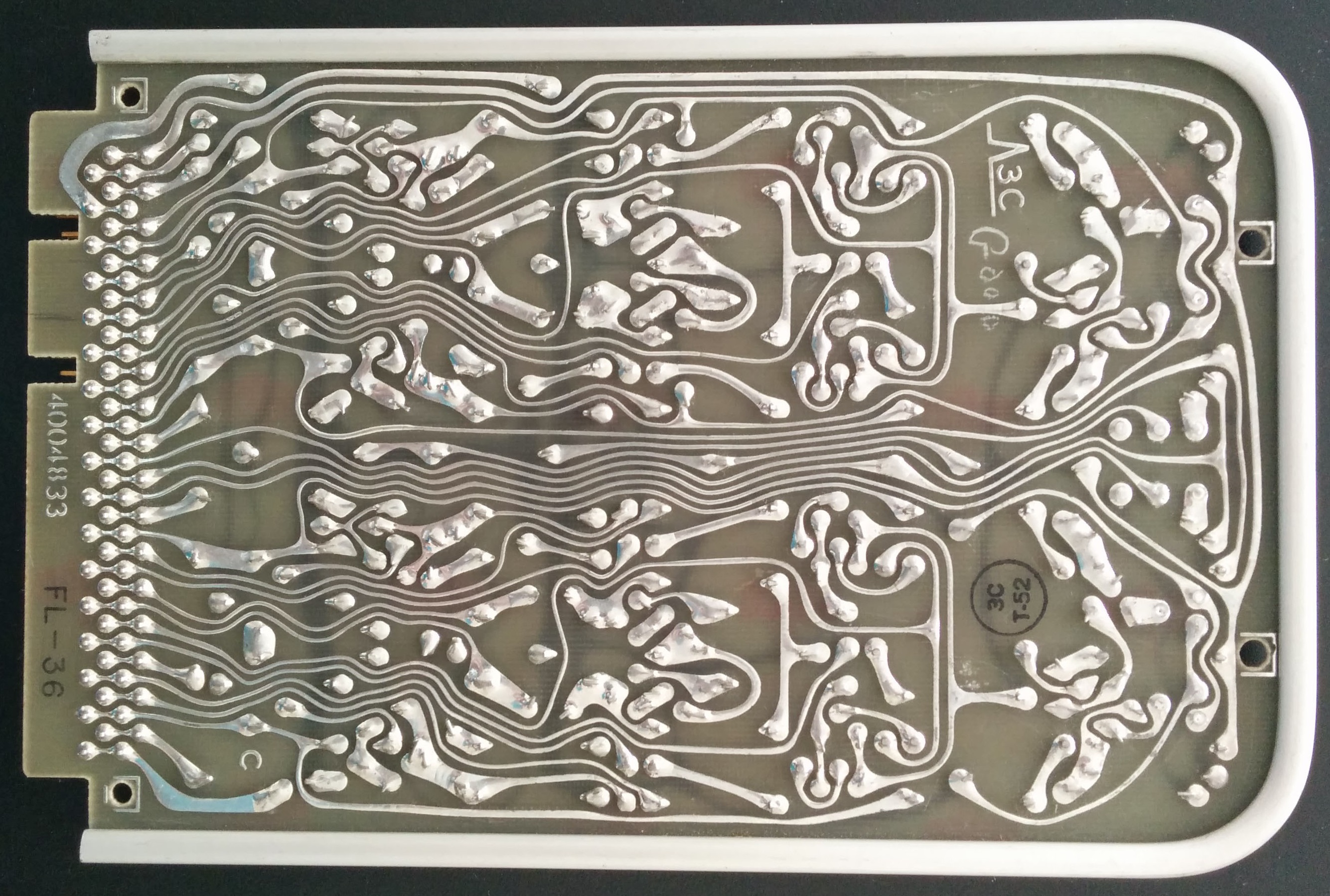
I think I can do that... PDF of instruction manual and images of both sides of the PCB attached here.
Enjoy.
Jon.
Dekatron42
Aug 16, 2016, 6:10:31 PM8/16/16
to neonixie-l
Thanks Jon!
/Martin

MichaelS
Aug 16, 2016, 9:49:06 PM8/16/16
to neonixie-l
Thanks, Jon!
BTW - does anyone know of a source for connectors for these, or how to make one?

Terry S
Aug 17, 2016, 1:02:35 PM8/17/16
to neonixie-l
I just love looking at old PCB layouts. Hard to tell if this was a hand taped design or an early CAD design, likely taped because of the date. The schematic looks like CAD.
PCB design has come a long way. I've been doing it 30 years now. There are things done on these early PCBs that we avoid like the plague now.
Terry
On Tuesday, August 16, 2016 at 1:44:55 PM UTC-5, Jon wrote:

gregebert
Aug 17, 2016, 1:46:11 PM8/17/16
to neonixie-l
I'm certain it's a "tape-and-donuts" PCB layout. The first CAD-developed PCB's I saw in the 1980's had telltale 45-degree bends everywhere, and everything else was perfectly orthogonal.
Notice there are no traces going between 0.1"-spaced pads, due to the primitive manufacturing capabilities at that time.
Remember when they used to gold-plate everything ? Some were so thickly plated they appeared to be solid gold.
Terry S
Aug 17, 2016, 2:04:08 PM8/17/16
to neonixie-l
I am sure you are right -- notice some of the odd angles and mixed 45/90s. Also notice the very poor registration of the holes to pads.
Gold plating has been making a big comeback in recent years -- ENIG -- or electroless nickel immersion gold. It's a good finish for lead free solder. Almost everything I've done for 7 or 8 years now gets ENIG. At many board houses it's not even a premium cost adder. It's a soft finish -- not suitable for edge connectors.
Terry

John Rehwinkel
Aug 18, 2016, 1:04:54 AM8/18/16
to neoni...@googlegroups.com
> In the early 80's I was doing 8 mil lines & spaces, getting two traces between pads on .1" spacing. It was pushing the limit of the local board houses. It was also just the ticket for high speed memory boards for a couple decades, until the DDR stuff came along. Now 6 mil is considered large, 4 mil is the bottom size without paying for low yields. I still use 8 mil on boards that can afford it, from a density standpoint.
I do 10/10 if it will fit, a lot of 8/8 and a few 6/6, but most of the stuff I design isn’t terribly tight.
> Gold plating has been making a big comeback in recent years -- ENIG -- or electroless nickel immersion gold. It's a good finish for lead free solder. Almost everything I've done for 7 or 8 years now gets ENIG. At many board houses it's not even a premium cost adder. It's a soft finish -- not suitable for edge connectors.
> PCB design has come a long way. I've been doing it 30 years now. There are things done on these early PCBs that we avoid like the plague now.
- John
Terry S
Aug 18, 2016, 8:04:29 PM8/18/16
to neonixie-l
John,
There's probably little I can teach you, it sounds like you are a seasoned designer as well. But for the group, here is some of what I see on the eval board that would not pass muster today.
1) Mid trace T's. Also off-angle T's in particular. These are frowned upon, especially in modern fine line designs. The T creates acid traps in the 90 degree corners. Much better to run traces out of and thru pads -- the round pad effectively opens the corner and "softens" the acid traps.
2) 90s. For the same reasons, 90s are generally avoided. Virtually every 90 can be done with 45s.
3) Pad exits at angles other than 45 or multiples thereof. It simply makes for inefficient routing resource usage. Again, critical in higher density designs. It's also ugly.
4) Pad exits off center from the pad. These create acute inside angles, acid traps. Also 45s and other angle bends too close to pad exits.
5) Diode symbols done in copper -- why? Almost no other component polarity is marked. Also the markings here are *under* the diodes -- not very useful. Copper is for current - and sometimes heat.
6) IC pin 1 marking. Let's use a square pad.
7) Routing not following the golden rule -- horizontal on one layer, vertical on the other. This is the rule you follow when routing, then break during optimization. You break it to reduce vias.
I could go on with what's wrong with the layout, but it's not really fair to compare this design to a modern CAD generated design. This was done when the tools didn't exist and iterations were difficult.
Regarding HASL -- I consider that finish obsolete. Like you said, ugly for lead free. Immersion Silver is a better option if you must avoid ENIG for cost reasons. I never liked HASL even in the lead solder days -- too often it caused the old glossy wet film solder masks to bubble & flake. But we used it.
Solder mask: The current standard is liquid photo-imageable. Dry film is also still popular.
Silkscreen: This is the subject of some controversy these days. Some designers subscribe to the new "eliminate the silkscreen for production" theory. I don't, but that's because I'm always the guy debugging the design, not just doing the layout. I want that silkscreen. I want it when I'm probing a board buried in a machine. I want it when a board comes back from the field with a burned spot... and I want it when it's rework time or UL testing time. I have never let my employer or client talk me into eliminating the silkscreen - yet. It's such a small cost adder in production, and believe me, your contract manufacturer (CM) likes to have it too.
Substrates: Too big a topic to cover here. But FR4 is obsolete.... there are a wealth of choices, consult your CM and engineers....
Terry S
CID

Roddy Scott
Aug 19, 2016, 2:49:00 AM8/19/16
to neonixie-l
A good time ago, I spent 10 years with a PCB producer as an equipment technician and saw everything from railroad tracks down to 4x4 tracking, from single sided to 24 multilayer boards, from boards for key fobs to guidance boards for Exocet in that time.
I had almost forgotten everything in regards to on design until your post. Thanks for the memory jog!

Alex
Aug 22, 2016, 4:42:57 PM8/22/16
to neonixie-l
I spin quite a few PCB designs at present where I work, using the latest incarnation of Orcad (very much a love / hate relationship). A few years ago when I was starting out at a (different) company with Orcad, I opted for "Arc" routing rather than the conventional 45/90 degree modes and had a wonderful time. It was never appreciated (I managed to avoid having to redo it at least) but the product using the board is still in production at a fab house many years later.
Pretty much agree on all of Terry's points though. Getting components in a nice even grid arrangement is always my OCD point, cant beat a matrix of 0603 parts on a board. I tend to keep the grids course until placed and then drop to 10 mil for routing... We tend to do prototypes and low volume though so run all our boards through Wurth in Germany, who do ENIG by default now. The boards look really pretty.
Still miss this era though:
- Alex
Message has been deleted
Dekatron42
Aug 26, 2016, 11:21:30 AM8/26/16
to neonixie-l
I cleaned the document that Jon had scanned so kindly and made a sual-page document which I have included here.
I also made some PCBs which I hope will arrive soon so that I can try the design, hopefully I didn't make any errors in the layout.
I spotted an error in the file so I deleted my previous message as I couldn't edit it.
/Martin
Reply all
Reply to author
Forward
0 new messages