Skip to first unread message

Steve Cousins
Jan 16, 2019, 5:43:09 PM1/16/19
to LiNC80
So here's my Z80 processor card...
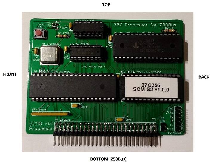
I've labelled the front and back as I intend it to be used, but is this the right way round?
I consider the front to be the side that faces me when I'm using it. I like my external connections to come out the back (note the serial port header). I like switches and lights to be on the front, facing me (note the reset button and indicator LED).
I intend making a range of cards and would like to find out now if my idea of front and back is considered correct.
Steve

Jon Langseth
Jan 17, 2019, 6:57:50 AM1/17/19
to LiNC80
The labels in your image are correct. The side with the connector is called the bottom. The side closest to Pin 1 (A15 signal) of the bus and perpendicular to the bottom is the back side, and should be used for connectors going in/out of a system. Connectors that will be serving system internal functions (i.e. would not require an externa connector on an enclosed system) may be placed at designers discresion.
For the LiNC80 SBC1, this makes the side with the power connector and "IDE" connection the Front side, the side with the serial headers and the logo the Back, and the Z50Bus connector on the Left side of the system board. The Sound Card is an example of an expansion having it's connector (the stereo jack) located at the Back edge of the expansion (see image below). I've elected to leave the DIP switches on the boards that have them on the back side, reminiscent of old ISA cards that had DIP switches for address/irq settings available on the back. That said, I really like your cards where that function is on the front side...
Also, it's cool to see this "sneak preview" of your SC118 processor card on the group!
/i/20829/products/2018-10-28T16%3A32%3A21.455Z-_DSC0174.JPG)
Reply all
Reply to author
Forward
0 new messages