Teensy 4 MIDI controller experiment

K7MDL

Steve Haynal
K7MDL


K7MDL

K7MDL
Mike Lewis
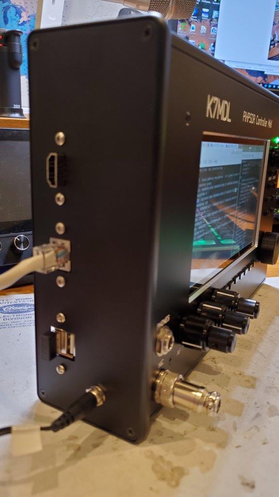
Exported a Step file from KiCAD and imported it into FreeCAD to generate this 3D. The 3 tall posts will be a vertical coin cell holder. This is facing front with the 4 pots and headphone jack on the far left. Teensy USB and the jacks on the back intended to set flush with a box back panel. The PCB size was not chosen for any special box, I made it as small as I figured I could reasonably squeeze everything in. The front pots are easy to separate and panel mount and wire if the chosen box is too deep. First time I have run this program. I have created a number of small PCBs over the year but the last time I did it professionally was on the late 80s with a 286 and EGA screen with a $15K P-Cad dongle attached, an big improvement of the hand taped layouts. Times have changed since then, cost have dropped to Free.

Mike
K7MDL EL87sm & CN88sf
Steve Haynal

Mike Lewis
No worries on updates. I just started this to learn KiCAD and maybe save wiring time on a proto board build, my usual approach, I will be following your build I the long run, or short tun if you end up routing sooner than later. These Teensy 4s are sitting on my desk, calling me, begging for something to do….
I will check out the parts sources you mentioned and start parts acquisition. Thanks for getting this started in your spare time. I am retired, I do this all day 😊.
Mike
K7MDL EL87sm & CN88sf
From: herme...@googlegroups.com <herme...@googlegroups.com>
On Behalf Of Steve Haynal
Sent: Tuesday, October 26, 2021 01:15
To: Hermes-Lite <herme...@googlegroups.com>
Subject: Re: Teensy 4 MIDI controller experiment
Hi Mike,
Nice to see you have placed and routed a board in KiCad! KiCad is quite the tool, especially for being open source.
The jacks are the same as used on the HL2 board. This is so makerfabs only has to source one part. See the HL2 BOM for an exact part number. You have to manually add a cutout on the circuit board for the front of each of those jacks as there is a plastic there that protrudes below the level of the PCB. See the HL2 layout.
The pots are a standard pinout and pin spacing. I think I bought several different brands in my last Digi-Key order. They are available from AliExpress too.
for example P160KN-0QC15B50K or any matching pinout.
1528-2164-ND are nice knobs on Digi-Key.
As I floorplan and layout a PCB, I often adjust the schematic to avoid wire crossings, pick other components to reduce footprint size, etc. For example, I reduced the size of the two test points. There have been several changes like this and I have updated github.
The wm8960 datasheet gives some PCB guidelines for the speaker outputs to reduce EMI. Components must be placed close to those pins. R33 is to terminate the clock and should be close to the wm8960.
I respecified a 2x5 connector so that the pinout matches the JTAG on the HL2. The HL2 JTAG can be used for fast communication, up to 30Mbs.
Sorry about this but I didn't know you were laying out a board! I just wanted you to be aware of new differences. Your board should still work although there may be minor differences in the pinout connections to the Teensy 4.0 which will have to be updated when building the firmware.
The 10cmx5cm size follows the 5cm increments for price increases that most PCB houses outside of the USA observe. Check out www.pcbshopper.com for places to have boards fabbed.
I don't know if we can use Teensy in the name. I remember seeing something about that somewhere but can't find it again on the prjc.com site.
KiCad has a 3D renderer builtin. Here is my board with components more or less placed. Next step is routing!
73,
Steve
kf7o

On Monday, October 25, 2021 at 8:14:49 PM UTC-7 K7MDL wrote:
Exported a Step file from KiCAD and imported it into FreeCAD to generate this 3D. The 3 tall posts will be a vertical coin cell holder. This is facing front with the 4 pots and headphone jack on the far left. Teensy USB and the jacks on the back intended to set flush with a box back panel. The PCB size was not chosen for any special box, I made it as small as I figured I could reasonably squeeze everything in. The front pots are easy to separate and panel mount and wire if the chosen box is too deep. First time I have run this program. I have created a number of small PCBs over the year but the last time I did it professionally was on the late 80s with a 286 and EGA screen with a $15K P-Cad dongle attached, an big improvement of the hand taped layouts. Times have changed since then, cost have dropped to Free.
Mike
K7MDL EL87sm & CN88sf

--
You received this message because you are subscribed to the Google Groups "Hermes-Lite" group.
To unsubscribe from this group and stop receiving emails from it, send an email to
hermes-lite...@googlegroups.com.
To view this discussion on the web visit
https://groups.google.com/d/msgid/hermes-lite/053e68e1-3745-425d-babd-fab66e821e2cn%40googlegroups.com.

Matthew
Mike Lewis
I did this one all by hand. That is why there are differences, for a quick proto, I was not applying all the best practices. I did use the DRC and fixed some traces that were too close. I thought I got rid of any stubs. I toggle the various layers to spot them by eye. I used only the defaults. 25 years ago I used to lay out high speed data acquisition boards, this is certainly not that level 😊. But this was done in hours, not weeks.
Mike
K7MDL EL87sm & CN88sf
To view this discussion on the web visit https://groups.google.com/d/msgid/hermes-lite/dc54d6c8-0885-4378-891d-3381e427bcc7n%40googlegroups.com.