Laser etched circuits

Alex Gibson
I am going to be laser etching some circuit boards very soon, to make Arduino shields and the like.
I may eventually put some on eBay if good enough, but the primary purpose is for fun and early prototyping ;)
Does anyone have experience of this, and would anyone like to join the party?
Unless it's possible to do this by lasering off the copper on the new laser (I think this would be hard to calibrate right), I expect to do it by spraying paint on the copper board as a mask, and lasering it off where I don't want tracks, using the Piranha laser cutter. I expect to get a step improvement in quality compared to acetate transfer methods. Amirite?
Cheers
Alex
Tapped on my mobile phone.

Stuart Livings
From the little I read about this a few years ago the issue is heat
conductance. The laser had a tendency to vapourise the painted mask
(which absorbed the heat just fine) but the real cutting energy was
wasted by diffusion and conductance by the copper.
I bow to the greatness of the laser gurus, of course...
Alex Gibson
The method I want to try is to paint a mask onto the copper PCB, and then laser it off wherever tracks aren't wanted. From there, normal PCB etching is done, it replaces the toner transfer stage, with hopefully better definition...
Tapped on my mobile phone.
> You received this message because you are subscribed to the Google Groups "Reading Hackspace" group.
> To unsubscribe from this group and stop receiving emails from it, send an email to reading-hacksp...@googlegroups.com.
> For more options, visit https://groups.google.com/d/optout.
>

Julian Johnson

Dale Strickland-Clark
Alex Gibson
Hi Dale,
Timing is pretty open – I am keen to get on with it, have the bits, but having had some deliveries of components I am busy knitting 3D printer parts and tweaking the tolerances for the first batch of machines.
What works for you? I can definitely do Wednesday evening, or for more peace and quiet I could do another evening or afternoon this week.
Cheers,
Alex
--
You received this message because you are subscribed to the Google Groups "Reading Hackspace" group.
To unsubscribe from this group and stop receiving emails from it, send an email to reading-hacksp...@googlegroups.com.
For more options, visit https://groups.google.com/d/optout.
No virus found in this message.
Checked by AVG - www.avg.com
Version: 2015.0.6081 / Virus Database: 4392/10309 - Release Date: 07/26/15

Richard Ibbotson
What are the plans for drilling ? Is the CNC mill working ?
What are your plans for etching ? Do you need to set up the etching kit in the fume cabinet ? I think the cabinet is still disconnected from the extractor fan. Need to make up new etchant and developer
Dale Strickland-Clark
Alex Gibson
Sounds good to me – 19:00 it is.
Anyone else want to join us?
Cheers
Alex
Dale Strickland-Clark
Alex Gibson
Shapeoko is working, but I don’t mind hand drilling these – dremel or drill press for better accuracy. This is a (hopefully working) proof of concept for me.
I will get there early and see about making up etchant etc, and see if I can reattach the fume cabinet – is this hard to do?
Richard Ibbotson
I think the Cookie Crew are down Tuesday too. May be a bit busy downstairs.
Alex Gibson
Cookie crew? Heard of this but no idea what it is. Like laser club but for biscuit lovers?

Andy Noyes

Matthew Daubney
Alex Gibson
Good idea, thanks for checking it out Matt
From: reading-...@googlegroups.com [mailto:reading-...@googlegroups.com] On Behalf Of Matthew Daubney
Sent: 27 July 2015 20:31
To: Reading Hackspace
Cc: al...@alexgibson.net

Mark Richardson
Alex Gibson
Yep, tomorrow at 7.
This is my first attempt too using this method – so we will see what happens!
Got any PCB material and/or boards you need to make?
From: Mark Richardson [mailto:mark.sp...@googlemail.com]
Sent: 27 July 2015 22:10
To: Reading Hackspace
Cc: al...@alexgibson.net

Alexander Hosford

Ian Petrie
Alex Gibson
Hi Alex, great to hear from you.
That’s valuable perspective – thanks. Especially the paints that worked and trick to deal with residue. I am surprised the resolution wasn’t great… for me that’s the point of trying it...
Echoing back to rLab membership – does anyone have strong objection to our using the laser cutter in this way tomorrow evening? I don’t expect us to do much tomorrow.
Is anyone aware of an ideal paint we could use to resist etchant but more completely vaporise by the laser?
I wonder about using adhesive sheet instead of paint?
Mark Richardson

Gary Fletcher
not sure if anyone else shall have an objection - but perhaps start on the small one..??
Alex Gibson
Yes – I was thinking that too…
I will be using Halfords or rustoleum matt black spraypaint for maximum lasering, and draw, not scan the gaps between traces, maybe even do both. I think this may be where some of the residue comes from.
From: reading-...@googlegroups.com [mailto:reading-...@googlegroups.com] On Behalf Of Gary Fletcher
Sent: 28 July 2015 00:34
To: reading-...@googlegroups.com
Subject: Re: [RDG-Hack] RE: Laser etched circuits
>>>Is anyone aware of an ideal paint we could use to resist etchant but more completely vaporise by the laser?

Barnaby
Barnaby
Btw. Once you have etched off the copper, you can laser cut the holes. Works best with FR1 but then all forms of drilling do. Also if you can drill more accurately then the CnC, then it is broken!

Richard / rgproduct
Alex Gibson
I will try varnish as well as paint,makes sense to me, and definitely consider cutting the holes - maybe need a jig to hold boards in the laser cutter.
Tapped on my mobile phone.
>
> It also occurred to me that you may be better with a varnish, they shouldn't have any trouble absorbing the huge amount of laser power, and are likely to vaporise more completely then the pigments.
>
> Btw. Once you have etched off the copper, you can laser cut the holes. Works best with FR1 but then all forms of drilling do. Also if you can drill more accurately then the CnC, then it is broken!
>
Alex Gibson
Hopefully there won't be any smoke and mirrors...
Tapped on my mobile phone.
>
> This thread sounds awesome. Missing 2 good things on tue night. Grr.
>
Alex Gibson
Thanks,
Alex
Tapped on my mobile phone.

Ryan .
Laser cut the holes??
Richard Ibbotson
Did Paul take his UV light box away ? Can also bring one down in case.
Alex Gibson
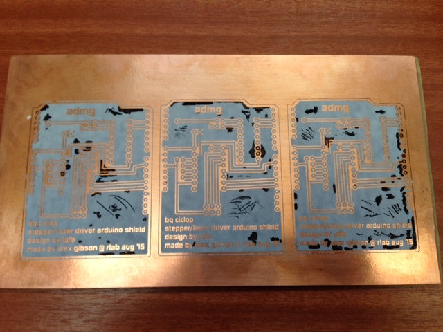
I want to share the results from yesterday's experiments making PCBs with laser etched paint as the etch resist.
We succeeded in the objective to test the process, but not in making a useful PCB, and there were a few issues along the way.
Gary Fletcher
Think i have a spare heater. Well done on the experiment, the cnc uv certainly sounds interesting!
> You received this message because you are subscribed to the Google Groups "Reading Hackspace" group.
> To unsubscribe from this group and stop receiving emails from it, send an email to reading-hacksp...@googlegroups.com.
> For more options, visit https://groups.google.com/d/optout.
>
>
> Here is a PCB sprayed with Halfords acrylic based car paint (Volvo grey), then etched by scanning at (allegedly) 200mm/s. I picked this one because I accidentally started on a cut setting - you can see it to the right.
>
> This was quite promising looking - it seemed to go very well. However, look at the small vias - they are way too fragile, there is overspill.
>
> Under magnification:
> --
> You received this message because you are subscribed to the Google Groups "Reading Hackspace" group.
> To unsubscribe from this group and stop receiving emails from it, send an email to reading-hacksp...@googlegroups.com.
> For more options, visit https://groups.google.com/d/optout.
>
> This was a relatively good bit.
>
> Notice that the resolution of the laser scanning is really too low for the find details we are trying to pick out.
>
> Also note the line pattern in the residue left on top of the etched pattern. This proved critical at the copper etch stage.
> --
> You received this message because you are subscribed to the Google Groups "Reading Hackspace" group.
> To unsubscribe from this group and stop receiving emails from it, send an email to reading-hacksp...@googlegroups.com.
> For more options, visit https://groups.google.com/d/optout.
>
>
> Here are 2 boards after spending ages in the etch bath. (Note the overlaid patterns are from repeated lasering using different settings)
>
> The one in the left had been coated with wood varnish rather than paint - this appeared to have the residue removed more cleanly.
>
> However both seemed to resist the etchant to an excessive degree. Only the right hand (car paint) etched away properly.
>
> I tried following a suggestion from the Ben Heck Show, where he apparently succeeded in this process, to wipe the board with acetone gently to remove the residue. However, possibly because I sprayed thinly and not long before the experiment, the paint just wiped off - and the residue was not reliably removed:
> --
> You received this message because you are subscribed to the Google Groups "Reading Hackspace" group.
> To unsubscribe from this group and stop receiving emails from it, send an email to reading-hacksp...@googlegroups.com.
> For more options, visit https://groups.google.com/d/optout.
>
> The patch of black to the right is the bare PCB fibreglass board...
>
> There are some things we could try to do differently:
>
> Use the white laser cutter
> Scan repeatedly at lower power for less spread but remove more residue
> Use only varnish, repeat the acetone wipe
> Paint the boards more thickly, a few coats maybe, and allow to cure for longer
>
> Personally I was motivated to try to find a more click and go way to make PCBs, and feel this is not it... I would prefer to make my next home brew PCB using toner transfer technique.
>
> However there may be a much better way to use lasers:
>
> UV laser mounted on an x-y gantry, scanning a pattern directly onto UV cured etch resist.
>
> This would be genuinely saving a step - toner transfer - and remove a step where manual application adds quality control issues.
>
> Process would be
> - unpeel backing
> - fire laser
> - straight into etch tank
> - remove after a more predictable period of time (UV exposure more controlled)
>
> I would be keen to try this method, and Mark has built a cool x-y gantry from photocopier bits - so maybe worth another experiment!
>
> Meanwhile I will be etching tonight so please can the fume cabinet be left where it is - I am heading over shortly...
>
> One apology to the group - the etch tank heater was broken at some point in the experiments. Not sure exactly how, but I struggled initially to submerge both it and the bubble pipe, so it may have got too hot and had thermal shock when submerged. This may also partly explain poor results, but I'm not sure it's relevant.
>
> Anyone have any reactions, ideas or questions coming from this?
>
> See you later
> Alex
>
>
> Tapped on my mobile phone.
>
Alex Gibson
Weirdly this didn’t come through with all text via my iPhone. 2nd attempt below. Gavin feel free to include for the website if desired…
Hi all,
I want to share the results from yesterday's experiments making PCBs with laser etched paint as the etch resist.
We succeeded in the objective to test the process, but not in making a useful PCB, and there were a few issues along the way.

Here is a PCB sprayed with Halfords acrylic based car paint (Volvo grey), then etched by scanning at (allegedly) 200mm/s. I picked this one because I accidentally started on a cut setting - you can see it to the right.
This was quite promising looking - it seemed to go very well. However, look at the small vias - they are way too fragile, there is overspill.
Under magnification:

This was a relatively good bit.
Notice that the resolution of the laser scanning is really too low for the find details we are trying to pick out.
Also note the line pattern in the residue left on top of the etched pattern. This proved critical at the copper etch stage.

Here are 2 boards after spending ages in the etch bath. (Note the overlaid patterns are from repeated lasering using different settings)
The one in the left had been coated with wood varnish rather than paint - this appeared to have the residue removed more cleanly.
However both seemed to resist the etchant to an excessive degree. Only the right hand (car paint) etched away properly.
I tried following a suggestion from the Ben Heck Show, where he apparently succeeded in this process, to wipe the board with acetone gently to remove the residue. However, possibly because I sprayed thinly and not long before the experiment, the paint just wiped off - and the residue was not reliably removed:

No virus found in this message.
Checked by AVG - www.avg.com
Version: 2015.0.6081 / Virus Database: 4392/10330 - Release Date: 07/29/15
Alex Gibson
Hi all,
Wanted to share some further experience as a relative newbie jumping in at the deep end of PCB prototyping and manufacturing:
Laser etched paint as etch resist:
Flush from my failure successful evaluation of laser stencilling PCBs with paint/varnish for DIY etch, I will be making a further effort at making my own prototype Arduino shields on Monday using toner transfer.
Toner transfer:
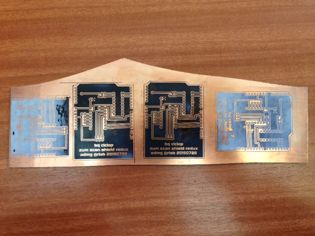
Attached is a photo of the stencilled board. I wonder which will come out best?
For all 4, I used a domestic iron on maximum heat to transfer toner that had been laser printed onto glossy photo paper. The board is plain copper, not UV cured.
Leftmost is a little extra one I cut down to use up space. I peeled off the paper here first, as an experiment, dry and immediately after heating with the iron. Even though this was part of the PCB I had not buffed with wire wool, I had cleaned the lot with Isopropyl Alcohol (IPA) and it stuck so well that the paper peeled off, leaving only toner and some residue from the gloss of the paper. I wonder if this will be the best, as the gaps between tracks are consistently clean copper, so should etch away well.
The other 3 I soaked the paper for some time before peeling off the majority and scrubbing away the residue with a sponge. Getting most of the paper off was easy, but the thin film of white residue proved trickier. The one on the right I deliberately left partially unscrubbed to see how badly it affects the etch – I assume it will be bad.
The two middle pieces came out better, and I scrubbed the residue away to the point that it is now shiny copper I can’t distinguish from plain PCB. Unfortunately some bits of the toner pattern came off. I believe this was not down to overzealous scrubbing, but instead due to poor adhesion to the copper.
I touched up both middle patterns with a Staedtler permanent CD/DVD marker pen. I don’t know if that will do the job – anyone have a known etch resist pen? I know they can be bought for the job – is a normal marker pen useless? I have seen Sharpies used.
Depending on results of this, a further area I will experiment with is different backing papers – I hear greaseproof paper is good, the wax coating makes sense to transfer well…
UV cured etch resist
I have previously made an Arduino shield at rLab using a circuit printed onto acetate – attached is a photo of a (perhaps the world’s only) dedicated shield to use Arduino as ISP to flash 40-pin ATMEGAs. If you’ve got a couple of hundred 644s or 1280s that need flashing, I got the tool for the job!
I think the UV exposure box went with Paul to Milton Keynes hackspace – do we have another? So far that seems the most repeatable process.
Getting China peeps to do it for me:
I’ve submitted orders to both PCBWay and Dirty Boards for a 3D scanner control board. This was pretty easy. I took published OSH designs and submitted them as a zip file.
PCBWay have a nice system that tells you exactly how your order is getting on. They evaluate your design in real time before taking your money, this was late Wednesday evening and I could see the updates in real time, it only took about 30 mins before I saw it had passed and they billed me via PayPal. Since, I have logged into my account and can see the progress – it’s 50% through the board house already – see below/attached J

Dirty Boards was mostly good, with a bit of a gotcha – after I submitted the gerber files, and had paid via PayPal, I got an error to say there was no board layout file (.GML). Oh no! I didn’t design the board and am not that intimate with Eagle etc, so I googled a copy/paste of the error message. Thankfully another newbie had encountered this and suggested I rename the .GM1 file to .GML - I did this, and Dirty boards’ system accepted the update and showed me a pretty picture of what my board should look like – which was nice, except the vias appeared to have solder in them, not empty? I have deliberately not attempted to tweak the design in any way.
Dirty Boards have good comms too – I signed up for tweets about progress, so they alerted me to the issue, and I got one early this morning to say the design is at the board house.
The whole point of this exercise for me was to evaluate the 2 services – so far, so good for both, I haven’t had any real panic, and there is reassuring comms. PCBway are a nose in the lead on price (50 cents cheaper) and speed so far, and I like the detailed breakdown of processes complete. But lots of hackspace people swear by Dirty Boards, I like the tweets and the preview picture. The real race is to my front door, and on quality. We’ll see!
I looked at alternatives – OSHpark is comparatively much more expensive and slower, but their purple boards do look awesome… anyone recommend an alternative?
Cheers,
Alex Gibson
+44 7813 810 765 @alexgibson3d 37 Royal Avenue, Reading RG31 4UR
admg consulting
· Project management
· Operations & Process improvement
· 3D Printing

Norro
Alex Gibson
Tapped on my mobile phone.

Gavin Gaunt
From: Alex Gibson
Sent: 31/07/2015 12:48
To: reading-...@googlegroups.com
Subject: Re: [RDG-Hack] RE: Laser etched circuits
Richard Ibbotson
Maybe if you properly install the fume cabinet and fix the broken etch tank, I could be more tolerant.
Ryan .
I have a UV exposure box and PCB shear, but am reluctant so leave at space, due to general disrespect of tools. Can bring down for one of events though.
Maybe if you properly install the fume cabinet and fix the broken etch tank, I could be more tolerant.
Richard Ibbotson
Hugo Mills
> Nah, the wholly you
That would be the Lamb of God?
Hugo.
--
Hugo Mills | In one respect at least, the Martians are a happy
hugo@... carfax.org.uk | people: they have no lawyers
http://carfax.org.uk/ |
PGP: E2AB1DE4 | John Carter, A Princess of Mars
Richard Ibbotson
Richard Ibbotson
No worries cobber , she's happy
Ryan .
Doh ! You meant the woolly yew
No worries cobber , she's happy
Hugo Mills
> https://www.youtube.com/watch?v=dulxbKkj9Wg
I was thinking of https://www.youtube.com/watch?v=nP4v7a8-pcU but
your version's good, too. :)
Hugo.
> On Fri, Jul 31, 2015 at 3:42 PM, Richard Ibbotson <
> richard....@btinternet.com> wrote:
>
> > Doh ! You meant the woolly yew
> > No worries cobber , she's happy
> >
--
hugo@... carfax.org.uk | forget
http://carfax.org.uk/ |
PGP: E2AB1DE4 | Welcome to Night Vale
Alex Gibson
I recently owned up to probably being responsible for breaking the heater in the etch tank, because in my first attempt to use it solo, I struggled to keep both the heater and the bubble tube under the etchant, as there was no obvious mechanism to make that happen, and I was being miserly with etchant. Gary has a spare and very kindly offered it as a replacement. I will be responsible for liaising with Gary to pick this up and getting it working, naturally.
When I came to experiment with etching I found the fume cabinet was a mess and effectively out of service because it had been moved to accommodate other projects, and it's no longer possible to get the extract hose underneath it. The fume cabinet is where it is right now so that it can be used - I'm back in on Monday to etch a circuit ahead of the TVRRUG meet. It's a 2-person lift and I'd struggle to move it safely alone so I hope it can remain there until then.
I've factored in time on Monday to work on re-connecting the fume cabinet to work in it by the sink permanently. If no-one objects that will likely mean making a big hole in the worktop. If I can do it without moving the chemical cabinet I will go for it alone, otherwise I may need a hand from anyone around.
A UV exposure box and PCB shears would be a real asset to the space. If left at the space, I'd propose that they and the etch tank were collected together with some PCB materials in a clearly marked box - one from the cupboard would be perfect - and live near the fume cabinet.
I am keen to do this to make the space work better, not as a quid pro quo, but if it helps you to feel more tolerant, so much the better :) I am grateful for the PCB materials you brought in recently, and your previous tutorial, which helped me to get going with this, and I am keen to maintain my current momentum for improving the space.
End speech. It probably wasn’t necessary, but my fingers needed the exercise before bed, and it is Friday after all :)
You received this message because you are subscribed to the Google Groups "Reading Hackspace" group.
To unsubscribe from this group and stop receiving emails from it, send an email to reading-hacksp...@googlegroups.com.
For more options, visit https://groups.google.com/d/optout.
Version: 2015.0.6086 / Virus Database: 4392/10348 - Release Date: 07/31/15
Ian Petrie
Alex
Please talk to me before fitting the fume cupboard.
When will you be at the space?
Ian
Alex Gibson
Tapped on my mobile phone.
Ian Petrie
I've given it some thought. I talked about it at the GM in February.
At the simplest it just needs blocking up to let the vent hose connect. I'd like to find a solution though that leaves the draining board clear. Possibly jacking the cabinet up in the air.
Alex Gibson
Tapped on my mobile phone.
I've given it some thought. I talked about it at the GM in February.
At the simplest it just needs blocking up to let the vent hose connect. I'd like to find a solution though that leaves the draining board clear. Possibly jacking the cabinet up in the air.
--
Richard Ibbotson
London seem to have locked up storage with restricted access for some tools, but is this a way we want to go ? Maybe if we press ahead with the personal storage, then some tools could be kept there and people ask if they want to use them ?
btw the air pump tube fits onto the side of the tank. There are holes in the bottom of the tank to aerate. The heater should be set to 60 degrees
Ian Petrie
I think we should discuss locked up storage for some tools. Particularly some hand tools which seem to be treated as trivial just because they don't have a plug on. I've got several tools which I'm not sharing because I know they would be abused, albeit innocently. My good tin snips for example and my best wood chisels.
Alex Gibson
Personal storage is a good idea, we have the boxes in the cupboard that should be used.
I think locking things up gets a bit cumbersome and prevents free choice of tools. But hey, if you are kind enough to loan or donate a tool and want some control over it, why not!
My view from watching the way things work in the space is that if we put some effort into clearly marking tools etc with their instructions, people do think about it more and keep things tidier. I'd like to believe whoever cut the cables with your original blade most likely did not realise it was an inappropriate use, and didn't differentiate it from more agricultural tools in the same area.
I'd suggest we simply put all the PCB stuff in one of the Really Useful Boxes, and I am ready and willing to make and laminate sheets showing the tool use instructions, and attach it to the bath, your guillotine if you are willing, etc. I really believe this will be enough to encourage the right behaviour.
What do you think?
Alex
Matthew Daubney
Richard Ibbotson
Matthew Daubney
Just dislike the idea of locking stuff away without a formalised method of training people to use them appropriately. Since you have the complaints, shouldn't it be you working to resolve them?
Richard Ibbotson
--
Matthew Daubney
Thats all. It's unfortunate, but sometimes it's the only way to change the underlying culture that causes the issue.
Matthew Daubney
Gavin Gaunt
From: Matthew Daubney
Sent: 01/08/2015 21:10
To: Reading Hackspace
Subject: Re: [Bulk] Re: [Bulk] RE: [RDG-Hack] RE: Laser etched circuits
Richard Ibbotson
Matthew Daubney
Well if you don't provide people a way to be able to use those tools, aren't you just turning the space into your own private workshop with your own tools locked away? How does that help contribute to sharing? If you want to preserve the tools you feel are important to you, and share them with others, surely you have to provide an onramp to that. Otherwise you're just arguing for storing your own tools in the space locked away from others. Which really doesn't encourage sharing.
Richard Ibbotson
Alex Gibson
Sidestepping any issues of people’s efforts being valued, and thinking only about sharing tools, I have a few simplistic thoughts:
1) It’s a scary thing to do, to share a tool of value to you, with a bunch of crazy hackers, only some of whom you know well.
2) It’s an awesome thing to enable a group to use something you have and only use 1% of the time, max
3) It’s hard when others have conflicting opinions as to what to do with something you have donated/lent and still feel ownership for
4) It’s worse when anyone’s motivations to do something get questioned. I basically like to assume they are all basically good, but from a different and weird perspective to my own weird perspective. I’d love others to assume the same of me.
5) Much of the stuff in the space got there because it was somebody’s rubbish. This includes some ludicrously valuable stuff, which is cool.
6) Some of the stuff in the space is of lower overt value, but represents a bigger stretch financially or emotionally to the donor/lender
7) None of this is a property of the tool itself, and cannot be expected of a visitor or new member. However it is reasonable to expect a basic level of respect for all items from all people. But what does this mean, when we are encouraged to use the tools, and have a go, using our own judgement.
8) It’s very hard to a new person in the space to know where something came from or what it is for, and certainly where it should be put away, unless it is clearly marked.
I believe there is a basic responsibility to treat all tools with respect. However I do think that if we lend an item to the space we should assume nothing about how valuable it appears to be, or that its intended use is obvious. I strongly believe that labelling will get us a long way with bridging this gap, it has already worked to improve how people treat several items. People can be expected to read and follow simple instructions like ‘this is a PCB cutter – do not use for other materials. If you want to use this and haven’t before, talk to Richard’.
End of my 2 cents.
From: reading-...@googlegroups.com [mailto:reading-...@googlegroups.com] On Behalf Of Matthew Daubney
Sent: 01 August 2015 21:26
To: Reading Hackspace
Matthew Daubney
It still comes down to the same problem of culture. By providing regular training sessions and/or workshops on equipment it helps people identify with their worth. It also allows new joining members an idea of when such sessions are running so they can be informed of the correct and safe use of such tools. It's a culture change you're trying to perform. You can just lock stuff away and ensure only certain members of a cabal can use them, but what you'll actually do is encourage the forming of factions within the community, which is obviously not the desired response.
The original base concept of the space is having members say "I don't think you're treating that tool with respect" or "I don't think you're working safely". To do that you have to reach a saturation point of knowledge within the base membership. Once you've reached that, then having the regular workshops and what not will start to encourage safe and practical use of said tools.
Of course, if you wish to start enforcing hard and fast rules with included punishments and what not, then it would be time to properly form an elected body to oversee the space in order to ensure that such rules are created and enforced fairly without undue bias. For the space to continue working as it is, but with more respect accorded to the tools, you have to change the culture.
Locking tools away and providing a consistant, regular onramp encourages that culture change. Locking tools away without providing that encourages faction forming. To do one, you have to do the other, otherwise we'll end up back here in 6 months time (which I expect we will anyway, because as we all know, these things just break down basically into people avoiding doing something and anyone who does anything is then stigmatised by others who don't agree with that action who will just ignore it anyway until it becomes useful to them).
As always with any tool you're using in the space, if you break it from neglect, it is expected that you repair/replace/manage the process of doing such to said tool. If it breaks from just wear and tear, then it is encouraged you do the same, but if the tool is loaned to the space from someone, then that is between the member and the others.
Alex Gibson
This is using toner transfer. I printed the reverse of the circuit onto inkjet photo paper with a laser b&w printer.
I then completed my minimal Ciclop shield yesterday.
As usual I obsessed over making it as tidy as possible, it was going to work, and it even looked great... Thanks to the black components on black board...

Yeah... I realised just before I attempted to sandwich it between an arduino and pololu to test, thanks to a comment from Tom, that the now neatly filed down edges clearly showed shiny layers of copper in the laminate. It is a 4 layer board...!
£@@&&&.
Goodness knows what it was doing with blank top and bottom surfaces in Richard's off cuts. I even suspected it and tried snapping the board to see, and thought it was not. Obviously, there are multiple shorts with the inner layers and the board is unusable.
I have now redone the toner transfer on a fresh single sided board. This time I peeled off the photo paper dry - again it went well, with minor retouching needed to bits where toner did not stick. Anyone got a top to improve adhesion?
I eagerly await the slow boats from China carrying my professionally made examples from PCBway and Dirty Boards...!
Alex
Tapped on my mobile phone.
Weirdly this didn’t come through with all text via my iPhone. 2nd attempt below. Gavin feel free to include for the website if desired…
Hi all,
I want to share the results from yesterday's experiments making PCBs with laser etched paint as the etch resist.
We succeeded in the objective to test the process, but not in making a useful PCB, and there were a few issues along the way.<image.jpeg>
Here is a PCB sprayed with Halfords acrylic based car paint (Volvo grey), then etched by scanning at (allegedly) 200mm/s. I picked this one because I accidentally started on a cut setting - you can see it to the right.
This was quite promising looking - it seemed to go very well. However, look at the small vias - they are way too fragile, there is overspill.
Under magnification:<image.jpeg>
This was a relatively good bit.
Notice that the resolution of the laser scanning is really too low for the find details we are trying to pick out.
Also note the line pattern in the residue left on top of the etched pattern. This proved critical at the copper etch stage.<image.jpeg>
Here are 2 boards after spending ages in the etch bath. (Note the overlaid patterns are from repeated lasering using different settings)
The one in the left had been coated with wood varnish rather than paint - this appeared to have the residue removed more cleanly.
However both seemed to resist the etchant to an excessive degree. Only the right hand (car paint) etched away properly.
I tried following a suggestion from the Ben Heck Show, where he apparently succeeded in this process, to wipe the board with acetone gently to remove the residue. However, possibly because I sprayed thinly and not long before the experiment, the paint just wiped off - and the residue was not reliably removed:<image.jpeg>
The patch of black to the right is the bare PCB fibreglass board...
There are some things we could try to do differently:
Use the white laser cutter
Scan repeatedly at lower power for less spread but remove more residue
Use only varnish, repeat the acetone wipe
Paint the boards more thickly, a few coats maybe, and allow to cure for longer
Personally I was motivated to try to find a more click and go way to make PCBs, and feel this is not it... I would prefer to make my next home brew PCB using toner transfer technique.
However there may be a much better way to use lasers:
UV laser mounted on an x-y gantry, scanning a pattern directly onto UV cured etch resist.
This would be genuinely saving a step - toner transfer - and remove a step where manual application adds quality control issues.
Process would be
- unpeel backing
- fire laser
- straight into etch tank
- remove after a more predictable period of time (UV exposure more controlled)
I would be keen to try this method, and Mark has built a cool x-y gantry from photocopier bits - so maybe worth another experiment!
Meanwhile I will be etching tonight so please can the fume cabinet be left where it is - I am heading over shortly...
One apology to the group - the etch tank heater was broken at some point in the experiments. Not sure exactly how, but I struggled initially to submerge both it and the bubble pipe, so it may have got too hot and had thermal shock when submerged. This may also partly explain poor results, but I'm not sure it's relevant.
Anyone have any reactions, ideas or questions coming from this?
See you later
Alex
Tapped on my mobile phone.
On 28 Jul 2015, at 18:33, "Richard Ibbotson" <richard....@btinternet.com> wrote:
I can bring some PCB laminate down.
Did Paul take his UV light box away ? Can also bring one down in case.
-----Original Message-----
From: reading-...@googlegroups.com [mailto:reading-...@googlegroups.com] On Behalf Of Alex Gibson
Sent: 28 July 2015 18:14
Subject: [Bulk] Re: [RDG-Hack] RE: Laser etched circuits
Hi, does anyone know where I could find spare PCBs at the space? I only had a little remaining and others coming tonight may want to try. Also the UV exposure chamber? I know they are downstairs somewhere...
Thanks,
Alex
Tapped on my mobile phone.
On 28 Jul 2015, at 12:07, Alex Gibson <al...@alexgibson.net> wrote:
Will post photos if we make anything decent, and confirm which methods hopefully worked...
Hopefully there won't be any smoke and mirrors...
Tapped on my mobile phone.
On 28 Jul 2015, at 10:22, Richard / rgproduct <rgpr...@hotmail.com> wrote:
This thread sounds awesome. Missing 2 good things on tue night. Grr.
--
You received this message because you are subscribed to the Google Groups "Reading Hackspace" group.
To unsubscribe from this group and stop receiving emails from it, send an email to reading-hacksp...@googlegroups.com.
For more options, visit https://groups.google.com/d/optout.
--
You received this message because you are subscribed to the Google Groups "Reading Hackspace" group.
To unsubscribe from this group and stop receiving emails from it, send an email to reading-hacksp...@googlegroups.com.
For more options, visit https://groups.google.com/d/optout.
--
You received this message because you are subscribed to the Google Groups "Reading Hackspace" group.
To unsubscribe from this group and stop receiving emails from it, send an email to reading-hacksp...@googlegroups.com.
For more options, visit https://groups.google.com/d/optout.
--
You received this message because you are subscribed to the Google Groups "Reading Hackspace" group.
To unsubscribe from this group and stop receiving emails from it, send an email to reading-hacksp...@googlegroups.com.
For more options, visit https://groups.google.com/d/optout.
No virus found in this message.
Checked by AVG - www.avg.com
Version: 2015.0.6081 / Virus Database: 4392/10330 - Release Date: 07/29/15
Ryan .
Alex Gibson
OK:
1) Point of the exercise is to learn through experimentation, evaluating the lowest hassle, most repeatable way to make PCBs with stuff we have at rLab and can use at home
2) The point of bothering at all is that boards from China take a few weeks, and breadboard is fiddly.
Many of us know much of this, I did from way back, but I’ve learned/consolidated that:
3) Laser removal of PCB etch resist looks shiny but sucks, because it is slower and less predictable than traditional methods, which don’t require a laser cutter
4) The classic homebrew way of making a circuit works well, and only needs an iron, a laser printer, and photo paper – I can do all the prep at home and then etch at rLab
5) We don’t need to get a UV exposure box and can skip a chemical stage
6) The specific technique of peeling the hot paper straight off works at least as well as soaking and rubbing off backing paper, takes no time and is less messy
7) Getting your PCB really clean matters, but you don’t need chemicals, just wire wool
8) so the process at home can be 100% dry, repeatable and hassle free
9) the fume cabinet back in use and the PCB making stuff is boxed, clean and ready to go.
10) I can reliably make usable quality single sided PCBs in about half an hour with only one chemical stage.
My next move is to try to make boards with the Shapeoko, hopefully in about 5 minutes.
Is it spam or of interest to anyone for me to describe what I do there and how it compares?
Cheers
Alex
Version: 2015.0.6086 / Virus Database: 4392/10363 - Release Date: 08/03/15
Hugo Mills
> 7) Getting your PCB really clean matters, but you don’t need chemicals, just wire wool
>
> 8) so the process at home can be 100% dry, repeatable and hassle free
dry process?
Hugo.
--
Hugo Mills | Great films about cricket: Forrest Stump
hugo@... carfax.org.uk |
http://carfax.org.uk/ |
PGP: E2AB1DE4 |
Ryan .
Ryan .
Alex Gibson
Yeah, crazy!
It was in an old stash of Richard's (no warranty asked or given).
It had solid copper on both sides, so I thought it was double sided.
I mentioned to several people the odd black pattern in the middle, and even roughly bent it to delaminate, it looked black and didn't conduct, so filed, I drilled and soldered up my board, loads of effort wasted! Tom spotted the filed edges had copper streaks before I toasted an Arduino at least.
I guess it must have been part of an aborted 4 layer process?
Alex Gibson
Got same result as wiping with IPA. I had buffed it nice and smooth. Maybe I would get better stick if liquid cleaned?

Stuart Livings
Did you get these boards back from PCBWay/DirtyPCBs? How do they look? What was the overall value of the commercial manufacturers?
Cheers,
Stuart
Hi all,
Wanted to share some further experience as a relative newbie jumping in at the deep end of PCB prototyping and manufacturing:
Laser etched paint as etch resist:
Flush from my
failuresuccessful evaluation of laser stencilling PCBs with paint/varnish for DIY etch, I will be making a further effort at making my own prototype Arduino shields on Monday using toner transfer.
Toner transfer:
Attached is a photo of the stencilled board. I wonder which will come out best?
For all 4, I used a domestic iron on maximum heat to transfer toner that had been laser printed onto glossy photo paper. The board is plain copper, not UV cured.
Leftmost is a little extra one I cut down to use up space. I peeled off the paper here first, as an experiment, dry and immediately after heating with the iron. Even though this was part of the PCB I had not buffed with wire wool, I had cleaned the lot with Isopropyl Alcohol (IPA) and it stuck so well that the paper peeled off, leaving only toner and some residue from the gloss of the paper. I wonder if this will be the best, as the gaps between tracks are consistently clean copper, so should etch away well.
The other 3 I soaked the paper for some time before peeling off the majority and scrubbing away the residue with a sponge. Getting most of the paper off was easy, but the thin film of white residue proved trickier. The one on the right I deliberately left partially unscrubbed to see how badly it affects the etch – I assume it will be bad.
The two middle pieces came out better, and I scrubbed the residue away to the point that it is now shiny copper I can’t distinguish from plain PCB. Unfortunately some bits of the toner pattern came off. I believe this was not down to overzealous scrubbing, but instead due to poor adhesion to the copper.
I touched up both middle patterns with a Staedtler permanent CD/DVD marker pen. I don’t know if that will do the job – anyone have a known etch resist pen? I know they can be bought for the job – is a normal marker pen useless? I have seen Sharpies used.
Depending on results of this, a further area I will experiment with is different backing papers – I hear greaseproof paper is good, the wax coating makes sense to transfer well…
UV cured etch resist
I have previously made an Arduino shield at rLab using a circuit printed onto acetate – attached is a photo of a (perhaps the world’s only) dedicated shield to use Arduino as ISP to flash 40-pin ATMEGAs. If you’ve got a couple of hundred 644s or 1280s that need flashing, I got the tool for the job!
I think the UV exposure box went with Paul to Milton Keynes hackspace – do we have another? So far that seems the most repeatable process.
Getting China peeps to do it for me:
I’ve submitted orders to both PCBWay and Dirty Boards for a 3D scanner control board. This was pretty easy. I took published OSH designs and submitted them as a zip file.
PCBWay have a nice system that tells you exactly how your order is getting on. They evaluate your design in real time before taking your money, this was late Wednesday evening and I could see the updates in real time, it only took about 30 mins before I saw it had passed and they billed me via PayPal. Since, I have logged into my account and can see the progress – it’s 50% through the board house already – see below/attached J

Dirty Boards was mostly good, with a bit of a gotcha – after I submitted the gerber files, and had paid via PayPal, I got an error to say there was no board layout file (.GML). Oh no! I didn’t design the board and am not that intimate with Eagle etc, so I googled a copy/paste of the error message. Thankfully another newbie had encountered this and suggested I rename the .GM1 file to .GML - I did this, and Dirty boards’ system accepted the update and showed me a pretty picture of what my board should look like – which was nice, except the vias appeared to have solder in them, not empty? I have deliberately not attempted to tweak the design in any way.
Dirty Boards have good comms too – I signed up for tweets about progress, so they alerted me to the issue, and I got one early this morning to say the design is at the board house.
The whole point of this exercise for me was to evaluate the 2 services – so far, so good for both, I haven’t had any real panic, and there is reassuring comms. PCBway are a nose in the lead on price (50 cents cheaper) and speed so far, and I like the detailed breakdown of processes complete. But lots of hackspace people swear by Dirty Boards, I like the tweets and the preview picture. The real race is to my front door, and on quality. We’ll see!
I looked at alternatives – OSHpark is comparatively much more expensive and slower, but their purple boards do look awesome… anyone recommend an alternative?
Cheers,
Alex Gibson
+44 7813 810 765 @alexgibson3d 37 Royal Avenue, Reading RG31 4UR
admg consulting
· Project management
· Operations & Process improvement
· 3D Printing
From: reading-...@googlegroups.com [mailto:reading-...@googlegroups.com] On Behalf Of Alex Gibson
Sent: 29 July 2015 20:24
To: reading-...@googlegroups.com
Subject: [RDG-Hack] RE: Laser etched circuits
Weirdly this didn’t come through with all text via my iPhone. 2nd attempt below. Gavin feel free to include for the website if desired…
Hi all,
I want to share the results from yesterday's experiments making PCBs with laser etched paint as the etch resist.
We succeeded in the objective to test the process, but not in making a useful PCB, and there were a few issues along the way.
Here is a PCB sprayed with Halfords acrylic based car paint (Volvo grey), then etched by scanning at (allegedly) 200mm/s. I picked this one because I accidentally started on a cut setting - you can see it to the right.
This was quite promising looking - it seemed to go very well. However, look at the small vias - they are way too fragile, there is overspill.
Under magnification:
This was a relatively good bit.
Notice that the resolution of the laser scanning is really too low for the find details we are trying to pick out.
Also note the line pattern in the residue left on top of the etched pattern. This proved critical at the copper etch stage.
Here are 2 boards after spending ages in the etch bath. (Note the overlaid patterns are from repeated lasering using different settings)
The one in the left had been coated with wood varnish rather than paint - this appeared to have the residue removed more cleanly.
However both seemed to resist the etchant to an excessive degree. Only the right hand (car paint) etched away properly.
I tried following a suggestion from the Ben Heck Show, where he apparently succeeded in this process, to wipe the board with acetone gently to remove the residue. However, possibly because I sprayed thinly and not long before the experiment, the paint just wiped off - and the residue was not reliably removed: