Help required on nixie power supply
165 views
Skip to first unread message

ZY
Jul 14, 2016, 1:03:26 AM7/14/16
to neonixie-l
Hello. I'm following desmith's guide to building a power supply, and I'm using a circuit somewhat similar to his except I've selected some different components due to some size constraints. The main difference is my mosfet is this guy: https://www.digikey.com/product-detail/en/toshiba-semiconductor-and-storage/TPH5200FNH,L1Q/TPH5200FNHL1QCT-ND/5456292
Anyway, my no-load output swings from 250V to 150V over the course of several seconds, during which there is no activity on the EXT pin. The output is basically just dropping due to leakage resistance. Once the output reaches 150V, I see switching activity on the EXT pin and the output quickly shoots up to 250V, and then switching activity stops again. This cycle just repeats. Putting a load of a single nixie on the output does not change the behaviour.
If I ground the FB pin, instead of seeing 12V at the output as expected I see something like 300-310V.
My FB pin usually sits around 1.7-1.8V as the voltage swings up and down. My Ref pin is at 1.5V as expected. My input voltage is 12V.
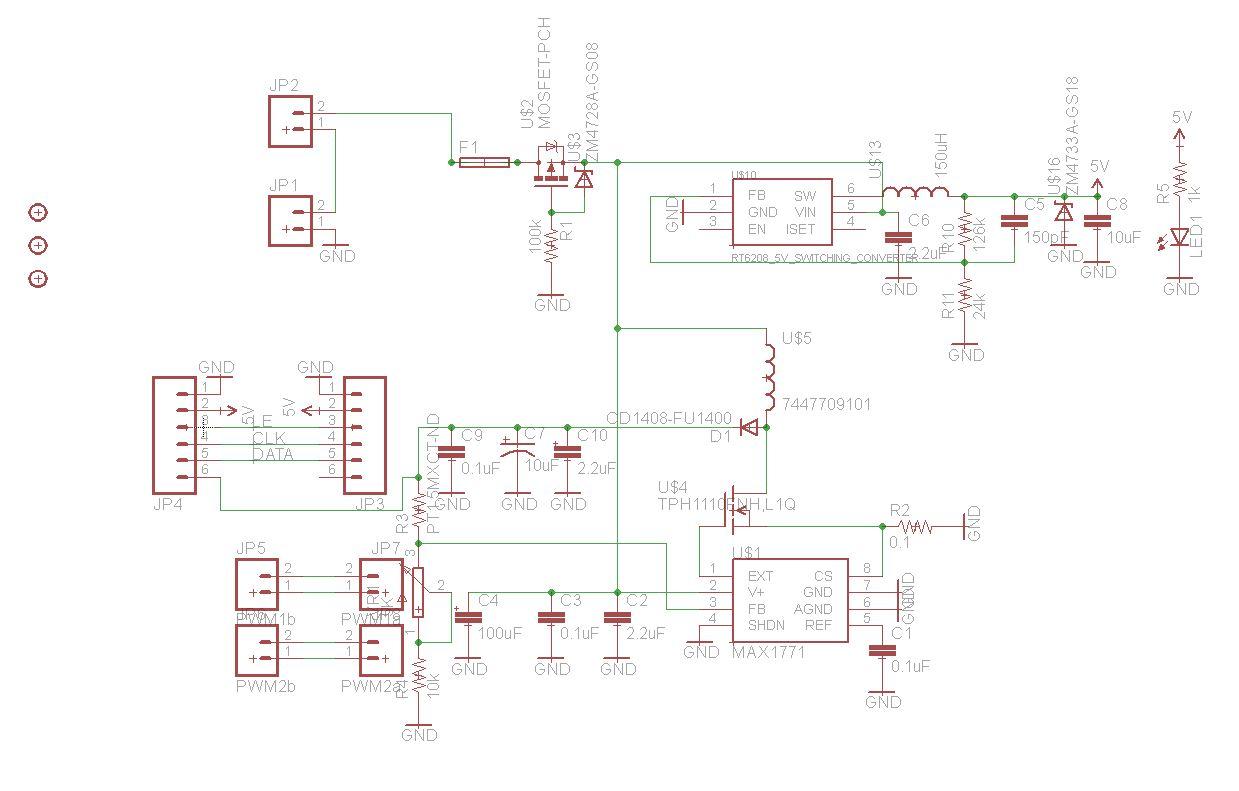
Can anyone give me some insight as to what is happening? I have attached a snippet of the circuit showing the HV supply portion.

SWISSNIXIE - Jonathan F.
Jul 14, 2016, 1:38:57 AM7/14/16
to neonixie-l
Have you tried to use a small capacitor 10-100pf on top of the resistor (the high value one, 1.5Meg or so) thats forming a voltage divider for the feedback?
This can really help.
What kind of output cap have you used?
This can really help.
What kind of output cap have you used?
ZY
Jul 14, 2016, 1:50:27 AM7/14/16
to neonixie-l
It seems like that is the issue. I can't find a suitable capacitor at the moment as the 0.1uF ones I have extra right now are rated at 50V, but using my multimeter to probe across the 1.5M cap causes enough parasitic capacitance to allow for a stable voltage output. I will order a similarly sized one as the resistor and solder it on top.
Also my output capacitors are a 10uF electrolytic capacitor, and a 2.2uF and 0.1uF ceramic capacitor, all three rated at 250V.
ZY
Jul 14, 2016, 1:58:15 AM7/14/16
to neonixie-l
Oops I meant 0.1nF for the capacitor across the 1.5M resistor, although I'm assuming 0.1uF would still be ok?
SWISSNIXIE - Jonathan F.
Jul 14, 2016, 6:56:24 AM7/14/16
to neonixie-l
I would try something between 10 and 200pf (0.01 and 0.2 nf). Anything more will maybe cause another problem. About the output cap, check its ESR, it will affect the overall performance. Also check if all solder-joints are in good quality.

gregebert
Jul 14, 2016, 10:51:36 AM7/14/16
to neonixie-l
Can you post a schematic ? I'm a bit concerned about the 250V-rated MOSFET, when you mentioned ~300V was measured. Is the MOSFET exposed to this voltage, or is there a doubler/tripler ?
My first guess is the supply is under-loaded, because the feedback mechanism is basically doing it job.
Secondly, I do wonder about the bandwidth of the feedback circuit. It's very possible the feedback pin is lagging the HV output. Can you measure the HV and FB waveforms on a scope ? Ideally you will want little or no lag (which is the case for a purely resistive divider); any filtering into the FB pin with a capacitor will introduce some lag as it creates an RC circuit.

John Rehwinkel
Jul 14, 2016, 11:25:38 AM7/14/16
to neoni...@googlegroups.com
> If I ground the FB pin, instead of seeing 12V at the output as expected I see something like 300-310V.
The input to the FB pin is proportional to the output voltage. If you ground it, it will see the output voltage as "too low" and try to raise it, giving the result you observed.
- John

Nick
Jul 14, 2016, 11:40:59 AM7/14/16
to neonixie-l
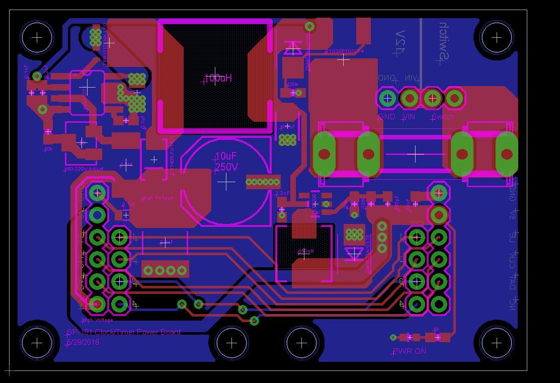
Can we see whole layout please?
Nick (de Smith)
ZY
Jul 15, 2016, 3:38:24 AM7/15/16
to neonixie-l
Thanks for all the responses:
I'm not sure about my ESR, I'm using this one: https://www.digikey.com/product-detail/en/nichicon/UUX2E100MNL1GS/493-9980-1-ND/3974089
which doesn't really list the value.
> I'm a bit concerned about the 250V-rated MOSFET, when you mentioned ~300V was measured. Is the MOSFET exposed to this voltage, or is there a doubler/tripler ?
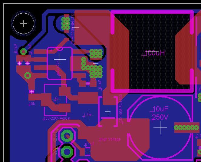
I have attached two images containing the board and schematics for this board. I apologies for my messy schematic layouts, I wasn't thinking anyone but myself was ever going to see this! There is no doubler or tripler. I too was surprised when nothing blew up during the short duration of 300V. The capacitors are also 250V rated. Maybe there's some factor of safety involved that preventing things from blowing up? I'm pretty sure my multimeter is accurate, as it is a good one from Fluke.
> My first guess is the supply is under-loaded, because the feedback mechanism is basically doing it job.
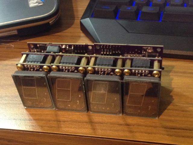
The power supply was intended to power 4 SP-101 displays, which would consume around 20mA if current if all the segments are on. I just tried a test with all my displays and the voltage does remain completely stable with all the segments lit. Unfortunately, not all the segments would be lit all the time, and if enough are off it starts to oscillate from 150-250V again.
> Can you measure the HV and FB waveforms on a scope ?
I'm not sure I can do this at the moment as my scope is a really cheap digital one and it can't do any HV. I'll have to get a voltage divider of some sort, but that may affect the measurements and I don't have access to any large high wattage resistors at the moment.
> The input to the FB pin is proportional to the output voltage. If you ground it, it will see the output voltage as "too low" and try to raise it, giving the result you observed.
That's what I thought it would do at first, but the datasheet says to connect to ground for fixed output operation? The fixed output mode circuit does use different components so I'm not entirely sure.
For the moment I think I'll order a 100pF and just place it overtop the 1.5M resistor as a quick fix. In my future designs I'll incorporate one next to the 1.5M resistor.
gregebert
Jul 15, 2016, 5:01:40 PM7/15/16
to neonixie-l
Although the supply is behaving like it's under-loaded, there could be another culprit: noise.
I've looked at the schematic, and it's possible that the PCB layout could be injecting excess noise into the MAX1771. Is the bypass cap C3 located as close to the 1771 as possible ? I think C4 should be close to the inductor. Be sure to check the power supply pins of the 1771 with your scope.
Nick de Smith
Jul 15, 2016, 11:42:00 PM7/15/16
to neoni...@googlegroups.com, gregebert
Noise on the FB pin is a common problem with poor layout, hence asking for a look at it.
You should not need any other bypass caps if the layout is good and the component choice likewise.
Nick
You should not need any other bypass caps if the layout is good and the component choice likewise.
Nick
On 15 July 2016 22:01:39 BST, gregebert <greg...@hotmail.com> wrote:
Although the supply is behaving like it's under-loaded, there could be another culprit: noise.I've looked at the schematic, and it's possible that the PCB layout could be injecting excess noise into the MAX1771. Is the bypass cap C3 located as close to the 1771 as possible ? I think C4 should be close to the inductor. Be sure to check the power supply pins of the 1771 with your scope.
--
Sent from my Android device with K-9 Mail. Please excuse my brevity.
Sent from my Android device with K-9 Mail. Please excuse my brevity.
ZY
Jul 23, 2016, 11:51:32 PM7/23/16
to neonixie-l, greg...@hotmail.com
Just an update. A 100pF cap over the resistor has indeed fixed the issue.
Noise on the FB pin is a common problem with poor layout, hence asking for a look at it.
I thought my layout would be ok. Maybe I'll remove the ground-plane keepout under the inductor next time as I'm using a shielded one to have less interruptions on the ground plane, and maybe I have to have a better 12V input to the IC. I thought my spacing and routing would be fine though, so I'm not sure.
gregebert
Jul 24, 2016, 2:39:31 AM7/24/16
to neonixie-l
Gad to see you got it running. Be sure to stress it over a wide range of supply voltages & load-currents to ensure it's robust. I also recommend probing around with a scope to make sure other signals are clean.
There are some good PCB-layout tips on the web for reducing noise. Many of them are not obvious at first-glance.
Reply all
Reply to author
Forward
0 new messages