OT: MOSFET in PWM application
87 views
Skip to first unread message

Tomislav Kordaso
Jul 22, 2016, 5:23:48 AM7/22/16
to neoni...@googlegroups.com
First, excuses for rather offtopic question. But knowing this fine group have excellent knowingly people, I'm posting the question here.
My circuit is employing P-MOSFET with its source connected to Vsupply, gate to microcontroller feeding PWM about 40 kHz, and resistive load connected between drain and GND. Effectively I have half of Vsupply at drain pin and everything is fine.If (via external circuit) Vsupply is briefly connected to load and drain pin, how this is going to affect MOSFET? I suppose this won't cause damage; can anyone point if my MOSFET is going to survive o long run or not? I tried it in my circuit and so far nothing bad can be seen.
I can not modify the behavior of external circuit so I have to live with this somewhat crude solution.
TIA
Tomislav

gregebert
Jul 22, 2016, 11:59:38 AM7/22/16
to neonixie-l
It would best if you could post a schematic.
Some things to be aware-of
1. Most, if not all, MOSFETS have a reverse-biased diode between source & drain. This needs to be considered during circuit design.
2. Vgs is breakdown is the easiest way to kill a MOSFET. I can't tell from the description what Vsupply is; if it's higher than the voltage supply to the microcontroller, you will have some design issues to fix.
Tomislav Kordaso
Aug 1, 2016, 9:35:23 AM8/1/16
to neoni...@googlegroups.com
Thanks, sorry for responding late, I was off the net for a while.
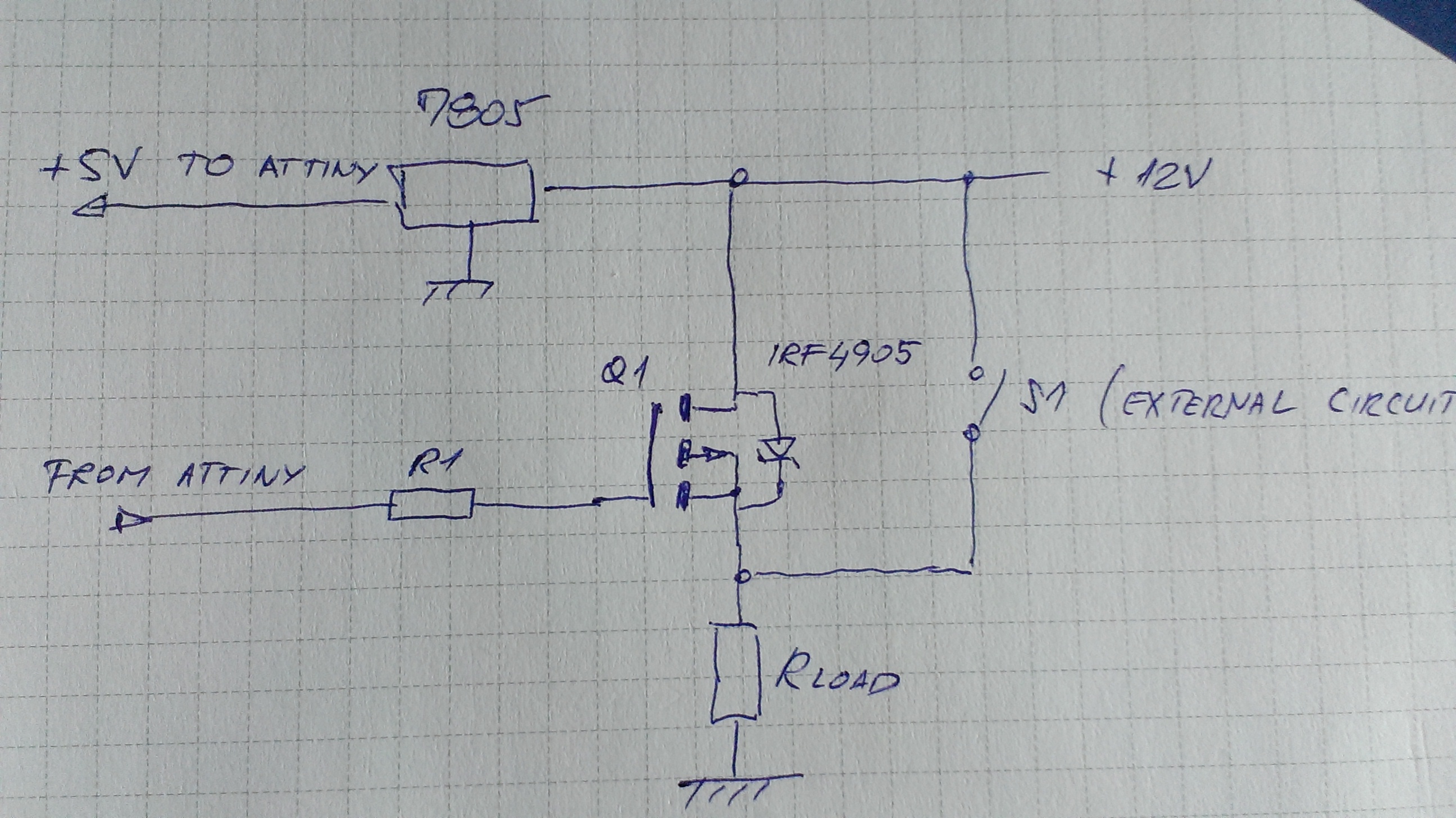
Attached is hand drawn schematic. Rload is about 2.4 Ohm. Circuit is working fine on test board, without external S1 being active.--
You received this message because you are subscribed to the Google Groups "neonixie-l" group.
To unsubscribe from this group and stop receiving emails from it, send an email to neonixie-l+...@googlegroups.com.
To post to this group, send email to neoni...@googlegroups.com.
To view this discussion on the web, visit https://groups.google.com/d/msgid/neonixie-l/9e45887e-1fff-4669-9ae0-0a7f60a51a75%40googlegroups.com.
For more options, visit https://groups.google.com/d/optout.
gregebert
Aug 1, 2016, 12:01:49 PM8/1/16
to neonixie-l
The way the schematic is drawn, Q1 is backwards, meaning the integral diode is feeding the load and the MOSFET has almost no control. Did you intend to have the source tied to your +12V supply ? I'm assuming yes, and you simply made a minor mistake in the drawing.
If your intent is to use the PMOS device to implement PWM on a resistive load, except when the switch is closed, you will need a 'high-side' driver that sets the gate to around +10 to +12V when the MOSFET is intended to be off. To turn the PMOS on, the gate needs to be around +8V or lower. Are you sure the ATTINY can drive those voltage levels ?
In any case, I dont see any obvious hazards with the switch; the Vgs rating for the MOSFET is 20V so you wont risk exceeding that running at 12V unless you have an inductive load.
BTW, this is a really high-power MOSFET so be aware of the leakage current.
Tomislav Kordaso
Aug 2, 2016, 3:30:30 AM8/2/16
to neoni...@googlegroups.com
I've made a fool of myself, sorry. Of course Q1 is drawn backwards.
Thanks for details provided, seems like I need some homework done.--
You received this message because you are subscribed to the Google Groups "neonixie-l" group.
To unsubscribe from this group and stop receiving emails from it, send an email to neonixie-l+...@googlegroups.com.
To post to this group, send email to neoni...@googlegroups.com.
To view this discussion on the web, visit https://groups.google.com/d/msgid/neonixie-l/55204026-8686-48f0-86dd-83126dd6feed%40googlegroups.com.
Reply all
Reply to author
Forward
0 new messages