H8 on a FPGA

56 views
Skip to first unread message

Les Bird

unread,
Sep 2, 2021, 5:58:12 PM9/2/21
to SEBHC
Hi all,

So lately (as in the last week) I've been obsessed with FPGAs. I have this little guy coming this weekend:

They are able to reproduce the hardware of arcade and console machines on a FPGA. For those that aren't familiar with FPGAs (I wasn't), it's a chip that has like 100,000+ logic gates built in and these gates can be rewired via software to emulate hardware. It's like designing and building out a PCB except if it doesn't work, you can fix it in software instead of sending off for more prototype boards. This is "hardware" emulation instead of "software" emulation.

I feel like an entire H8 computer can be built on a FPGA and I'm going to explore this when the MiSTer device arrives on Saturday. They already have cores for this gadget for a lot of popular computers. My thinking is that all the hardware such as the Z80 board and associated support chips can be wired on a FPGA chip and then installed into an H8 chassis (for front panel interfacing, etc). I don't know, seems like it could work. Additionally there should be no reason why we can't also have H17 and H8-4 hardware built on FPGAs as well.

Anyone have any thoughts? I mean, an H8 on a chip would be super cool.

Les

Douglas Miller

unread,
Sep 2, 2021, 6:51:42 PM9/2/21
to se...@googlegroups.com

"...and then installed into an H8 chassis" ... or in an Altoids tin...

I had thought about this to reproduce another pet-project of mine, the Honeywell 200/2000 mainframe computer. But for that there is very little detail on the hardware implementation. In that case, I would have wanted it to be a true implementation of the original hardware, to answer questions about how the CPU actually worked.

Last time I worked with FPGAs, 20 years ago, they had to be programmed via JTAG. These days I think it's easier, and I believe they even have non-volatile programming now. There are tools for converting things like VHDL (hardware description language) into FPGA programs, which is probably the best way to implement it (analogous to having source code and compiling it). There may be VHDL available for some of the ICs as well, although it may be easier to simply write (most of) the H8 "simulation" as VHDL.

Cool idea, but I have no clue about the practicality of it. I've always wanted to get into making my own FPGAs.

--
You received this message because you are subscribed to the Google Groups "SEBHC" group.
To unsubscribe from this group and stop receiving emails from it, send an email to sebhc+un...@googlegroups.com.
To view this discussion on the web visit https://groups.google.com/d/msgid/sebhc/aab8de6c-ac20-4b15-8a49-3a203651b87bn%40googlegroups.com.

Mark Garlanger

unread,
Sep 2, 2021, 9:02:13 PM9/2/21
to se...@googlegroups.com
Hey Les,

    A friend of mine built a z80 with an FPGA - https://github.com/gdevic/A-Z80  It may be a good starting point.

For things like serial ports and floppy drive controllers, won't you still need a bunch of supporting driver chips?

Mark


Les Bird

unread,
Sep 2, 2021, 9:26:41 PM9/2/21
to SEBHC
Very cool. Thanks Mark.

And yes to hook into real hardware we’d most likely need supporting chips I think.

Les


Les Bird

unread,
Sep 2, 2021, 10:06:35 PM9/2/21
to SEBHC
Douglas,

That Honeywell system sounds like it'd be a cool FPGA project. Let me know if you pursue that project.

So the MiSTer project is based on this FPGA dev board:

Base price is $170 and it includes a lot of interfacing options and GPIO pins. It is programmed via USB.

Les

PRL-89

unread,
Sep 3, 2021, 10:04:18 AM9/3/21
to SEBHC
Hi Les,

Seems everyone is building vintage stuff on FPGA’s these days.

Me, I’m finishing up the design for building an “almost” Z80 on breadboards using discrete components.

Yes, I know.  Insane.

Paul


Dave McGuire

unread,
Sep 3, 2021, 10:29:49 AM9/3/21
to se...@googlegroups.com
On 9/3/21 10:04 AM, PRL-89 wrote:
> Me, I’m finishing up the design for building an “almost” Z80 on
> breadboards using discrete components.

That's fantastic, you should move it to PCBs if you get it running.
Either way I'd love to see pics and more info.

> Yes, I know.  Insane.

I would say "wonderful", but that's just me.

-Dave

--
Dave McGuire, AK4HZ
New Kensington, PA

Les Bird

unread,
Sep 3, 2021, 11:02:18 AM9/3/21
to SEBHC
I agree with Dave, fantastic! Building a CPU using discretes is beyond me. Would love to see the results.

I get that FPGAs takes the fun out of building PCBs but it's new to me and I'm very intrigued with the idea and want to explore it.

Les

PRL-89

unread,
Sep 3, 2021, 11:46:02 AM9/3/21
to SEBHC

Thanks Dave!

I’ll post my design spec when it’s in better shape.

My “P80” breadboard Z80 is inspired by Ben Eater’s 8-bit CPU.  Ben posted a series of excellent YouTube videos showing in detail how he designed and built each of his CPU modules.  In all Ben used fourteen 830-pt breadboards for his CPU. (plus some +/- power rails for his 8-bit bus).  His CPU is very simple — 4-bit opcodes, 16 bytes of memory, two 8-bit registers plus a 4-bit PC register, an 8-bit data bus, and an ALU that does add and subtract.  It also includes an output register with 7-segment displays to display decimal 8-bit values.

I said “insane” because I want to build something closer to a Z80, with 64K of memory, all of the Z80 registers, separate 8-bit data and 16-bit address busses, (non-maskable) interrupts, and most of the Z80’s instruction set.  It will be opcode compatible (unsupported Z80’s opcodes generate NOPs).  The design spec details what Z80 features are included and what’s missing.

The P80’s expected size is around 17” x 17”. I’ll mount it on a wall.

I also relied heavily on Ken Sherriff’s work in reverse-engineering the Z80’s die, revealing much more about the Z80’s architecture and inner workings than Zilog ever did.

One significant limitation of the P80 compared to the Z80’s is that it is self contained, with its own 64K memory, input and output registers, etc.  There’s currently no external interface for connecting external devices like keyboards, monitors, etc.  The exception is a program interface that will let you connect an Arduino or other microcontroller and download program binaries via the controller’s USB serial port.

Since the P80 is binary compatible with the Z80, I should be able to use any existing Z80 (or 8080) assembler to create the P80’s binaries.

The P80 currently uses five 256K x 8 EEPROMs as its controller/sequencer, generating the 40 control signals that drive all of its actions.

I have no idea at this point if what I’ve designed is even feasible to build.  I’ve bought most of the ICs I need (50 of ‘em and counting), but that’s as far as I’ve gotten.

Going the route of PCBs would might actually be easier to build than using breadboards (a significant “rats nest of” wires).  But one of the appeals of Ben Eater’s breadboard CPU (and it’s many spin-offs) is all those LEDs scattered around his breadboards, turning an otherwise boring CPU into a “work of art”.

Performance is not one of my goals, but I’m designing the P80 with the goal of it being able to run at 1 MHz.   My design shortens some of the Z80’s instructions (e.g., the P80 uses an 8-bit ALU; the Z80’s ALU is only 4-bits), so some P80 instructions will require fewer clock cycles.  The P80 doesn’t have the Z80’s overlapped execute/fetch feature, so that puts the P80 at a performance disadvantage. 

Perhaps a single, very-large motherboard PCB that retains all of the LEDs would work.  But such a PCB might cost a small fortune to manufacture.

Once I post the design spec, I’ll be anxious to hear back from you or anyone else who might be able to comment on the feasibility of turning my design into something real, and offer any tips or guidance for moving forward (I’m a software guy by trade; my hardware skills are suspect).

Paul

On Friday, September 3, 2021 at 10:29:49 AM UTC-4 mcg...@neurotica.com wrote:

PRL-89

unread,
Sep 3, 2021, 11:50:21 AM9/3/21
to SEBHC
Les, I absolutely agree!  FPGA’s open a whole new world for those of us interested in vintage CPUs and computers.

The idea of an H8-on-a-chip (or H89-on-a-chip) is wildly intriguing!

Paul

Dave McGuire

unread,
Sep 6, 2021, 2:00:40 PM9/6/21
to se...@googlegroups.com

This sounds absolutely fantastic. If you distill this down to a PCB
layout (or several), I'd definitely put one together.

-Dave
> --
> You received this message because you are subscribed to the Google
> Groups "SEBHC" group.
> To unsubscribe from this group and stop receiving emails from it, send
> an email to sebhc+un...@googlegroups.com
> <mailto:sebhc+un...@googlegroups.com>.
> To view this discussion on the web visit
> https://groups.google.com/d/msgid/sebhc/88e4f3be-cee3-4828-9fdf-b55cdeac3f74n%40googlegroups.com
> <https://groups.google.com/d/msgid/sebhc/88e4f3be-cee3-4828-9fdf-b55cdeac3f74n%40googlegroups.com?utm_medium=email&utm_source=footer>.

Rob Doyle

unread,
Sep 6, 2021, 3:37:21 PM9/6/21
to se...@googlegroups.com

If you want to learn about FPGA, this is an excellent way to start.

The Terasic DE10-Nano (FPGA board used by MiSTer) will easily support an
H8 design including all of the goodies. Probably 10 of them or more.

I've used the DE10-Nano to build a Digital Equipment Corp KS10 36-bit
mainframe-ish computer with all the peripherals. The CPU is implemented
close-enough to the original to execute the original DEC microcode. I do
have an external 4 MB Synchronous SRAM (1 MW x 36) but everything else
is on-chip. This includes a disk controller for 8 washing machine sized
disk drives (storage is an SD Card), a tape controller for 8 tape
drives, a terminal multiplexer for 8 terminals, a communications
co-processor, high-speed synchronous communications adapter, printer, etc.

I've generated about 33,000 lines of verilog code and I still have used
only 29 percent of the logic cells and 9 percent of the on-chip memory.
The CPU and peripherals pass most of the DEC diagnostics.

https://github.com/KS10FPGA/KS10FPGA/wiki

If you need help or get stuck, help is probably lurking nearby.

Rob.
> --
> You received this message because you are subscribed to the Google
> Groups "SEBHC" group.
> To unsubscribe from this group and stop receiving emails from it, send
> an email to sebhc+un...@googlegroups.com
> <mailto:sebhc+un...@googlegroups.com>.
> To view this discussion on the web visit
> https://groups.google.com/d/msgid/sebhc/aab8de6c-ac20-4b15-8a49-3a203651b87bn%40googlegroups.com
> <https://groups.google.com/d/msgid/sebhc/aab8de6c-ac20-4b15-8a49-3a203651b87bn%40googlegroups.com?utm_medium=email&utm_source=footer>.

Les Bird

unread,
Sep 6, 2021, 4:20:55 PM9/6/21
to SEBHC
Wow Rob, that sounds fantastic. And good to hear the DE10 Nano can handle the H8 and extras. I wasn’t sure if it would be enough. Verilog is quite confusing to me right now. I’m looking through as much sample code as possible to try and understand it. I was hoping I could layout a schematic and then upload that but doesn’t seem to work that way.

Thanks for chiming in, this is reassuring.

What I’m hoping to do is have the CPU, H17, H37, H19 and H8-4 (and bonus HA-8-3 color graphics) all on the chip. Bonus would be hooking into real floppy drives via the GPIO pins. Since the H17 and H37 would be on the chip it’d be real cool to auto-detect the floppy disk, whether it be hard sector or soft then switch to the appropriate controller on the fly.

But first step is to boot to the ROM, then move forward from there.

Les

Rob Doyle

unread,
Sep 7, 2021, 8:57:25 PM9/7/21
to se...@googlegroups.com

It is my opinion that if you can draw schematics using 74xx chips - that
is the hard part.

Writing verilog is mostly just learning how to code a D flip-flop,
multiplexers, decoders, counters, shift registers, and combinational
logic. Once that is understood, you get an occasional FIFO, memory,
adder, or state machine.

Perhaps the most complicated thing is learning how the tools work. I
tend to script everything (unix makefiles) so I don't have to push
buttons on a GUI. With a single command, I can rebuild the firmware and
load it into the FPGA.

The verilog simulators work very well. I have a testbench wrapped
around the KS10 that provides simulated peripherals. For example, I
mentioned that the disk controller stores data on a SD Card. The
testbench has a simulation model for the SD Card that stores data on the
PC. The testbench also simulates memory and has a partial model for
RS-232 terminal. I can boot the CPU, the disk controller interacts with
the SD Card simulation and can read executables from my PC, I can watch
the CPU execute instructions, see RS-232 IO on a window, and can look at
any signal in the FPGA on something that looks like a 10,000 channel
logic analyzer.

Debugging on target hardware can be a little complicated. I added
breakpoint hardware into the CPU. It can stop the CPU on instruction
fetches, memory reads, memory writes, IO reads, and IO writes to an
address. I can read or write the internal registers. It also has an
instruction trace buffer which records the program counter in a large
FIFO - for traceback - which answers the age-old question: How did I get
here? These are all things that a Z80 could never do...

Rob.
> <https://groups.google.com/d/msgid/sebhc/aab8de6c-ac20-4b15-8a49-3a203651b87bn%40googlegroups.com?utm_medium=email&utm_source=footer
> <https://groups.google.com/d/msgid/sebhc/aab8de6c-ac20-4b15-8a49-3a203651b87bn%40googlegroups.com?utm_medium=email&utm_source=footer>>.
>
>
> --
> You received this message because you are subscribed to the Google
> Groups "SEBHC" group.
> To unsubscribe from this group and stop receiving emails from it, send
> an email to sebhc+un...@googlegroups.com
> <mailto:sebhc+un...@googlegroups.com>.
> To view this discussion on the web visit
> https://groups.google.com/d/msgid/sebhc/e5c678de-7d3f-4657-9993-b60ff8e960b0n%40googlegroups.com
> <https://groups.google.com/d/msgid/sebhc/e5c678de-7d3f-4657-9993-b60ff8e960b0n%40googlegroups.com?utm_medium=email&utm_source=footer>.

Norberto Collado

unread,
Sep 7, 2021, 10:29:38 PM9/7/21
to se...@googlegroups.com

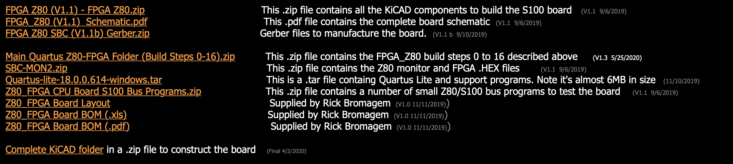
There is an article with introductions to FPGA that uses the Altera FPGA to create a Z80 that can be run at 50MHz. Perhaps something can be leverage to make this easier as it provides everything.


http://www.s100computers.com/My%20System%20Pages/FPGA%20Z80%20SBC/FPGA%20Z80%20SBC.htm


Norberto


Text

Description automatically generated

    To unsubscribe from this group and stop receiving emails from it, send an email to sebhc+un...@googlegroups.com.

    To view this discussion on the web visit https://groups.google.com/d/msgid/sebhc/71ef4e94-184d-87d6-2fbe-9e359edc0eb4%40gmail.com.

George Farris

unread,
Sep 7, 2021, 11:11:23 PM9/7/21
to se...@googlegroups.com
Just a warning, this is NOT a plug and play solution.  I have a close friend that bought one and he has experienced random crashs in the Z80 code and memory corruption in test routines.  Be prepared to spend many hours with this and possibly come out with a piece of hardware that isn't reliable.

It seems the Z80 code is rather half baked or maybe more like 8/10ths baked.

I can have him  email anyone that is interested.

Cheers
George

Les Bird

unread,
Sep 8, 2021, 8:01:43 AM9/8/21
to SEBHC
The Z80 core I was planning on using was the one that is part of the MiSTer project called the T80. It seems very stable as it is used in all of their cores for arcade games (Pacman, etc) and all of their computer cores such as the TRS80 and ZX Spectrum.

I'm hoping I can take an existing working computer core and modify it to simulate the H8. I think once I do that I'll have a better understanding of how things work and then can work on a system from scratch.

Rob, thanks for the tips. Good to know.

Les


Reply all
Reply to author
Forward
0 new messages