H8-512KB of RAM

Norberto Collado
Hello Douglas,
I will start working on the 512KB RAM board for the H8 to support CP/M3. Hopefully I can order some this week to test it out.
Thanks,
Norberto

Douglas Miller
Great! I hope testing goes smoothly. FYI, the software assumes MMU port is 00H. Keep me posted.
--
You received this message because you are subscribed to the Google Groups "SEBHC" group.
To unsubscribe from this group and stop receiving emails from it, send an email to sebhc+un...@googlegroups.com.
To post to this group, send email to se...@googlegroups.com.
To view this discussion on the web visit https://groups.google.com/d/msgid/sebhc/453D5800-BC89-4516-8A06-C25E1A3767E2%40koyado.com.
For more options, visit https://groups.google.com/d/optout.

Lee Hart
> Great! I hope testing goes smoothly. FYI, the software assumes MMU port
> is 00H. Keep me posted.
Douglas, I've never used a multi-user or multi-tasking networked CP/M
system. Could you perhaps explain why one would want to use one in an H8
or H89 where there is only one user, one computer, and you're unlikely
to have more than one job going at a time?
I don't understand the problem that the complex bank switching setup is
intended to solve.
--
Obsolete (Ob-so-LETE). Adjective. 1. Something that is simple,
reliable, straightforward, readily available, easy to use, and
affordable. 2. Not what the salesman wants you to buy.
--
Lee Hart, 814 8th Ave N, Sartell MN 56377, www.sunrise-ev.com

Peter Shkabara
I don't know if I am jumping in at the wrong point, but I assume you are referring to MP/M. When I got my H89 way back when, I soon got to know other computer owners in town. One of them had an S100 based system running MP/M with three terminals attached. He was the only user, but did use the multiple terminals much the way we now use multiple windows in a windows based computer. For instance, he might start a sorting job that would take a long time to run. He could then use another terminal to copy some files for me. It was not networking, but multi-tasking. I was certainly impressed then.
Peter Shkabara
Kol...@gmail.com
You received this message because you are subscribed to the Google Groups "SEBHC" group.
To unsubscribe from this group and stop receiving emails from it, send an email to sebhc+un...@googlegroups.com.
To post to this group, send email to se...@googlegroups.com.
Douglas Miller
(spawned/managed from a single console), but I could be remembering wrong.
The networking (CP/NET) is a separate thing. MP/M made a good network
server because of the multitasking... each network client had it's own
"environment" on MP/M. Digital Research, and probably others, also used
things like PDP/11s to run as CP/NET servers. The CP/NET clients are
single-user systems running (typically) CP/M as their base OS.
I think the main purpose of the H8-512K is to run CP/M 3, which is
single user but performs much better than CP/M 2.2 by leveraging the
extra memory (and has some new features). We could also work on an MP/M
port as well, although I'm not sure how much demand there would be.
Norberto Collado
Douglas,
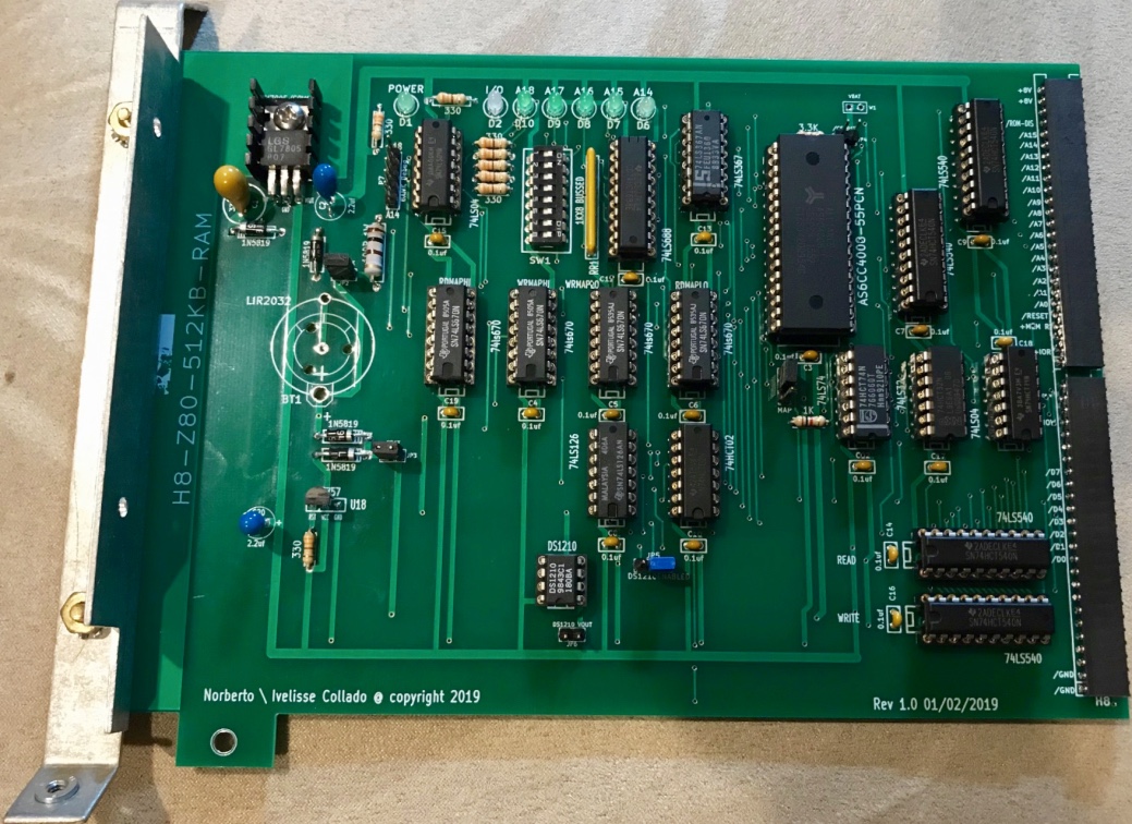
I ordered the H8-512KB RAM board. I used your schematics with some minimum HW changes to support battery backup and LED’s on the banks for trouble shooting. As you mentioned that such circuit is working on your emulator, I just went ahead and placed the order for three boards to verify for layout issues.
Thanks,
Norberto
From: "se...@googlegroups.com" <se...@googlegroups.com> on behalf of Douglas Miller <durga...@gmail.com>
Reply-To: "se...@googlegroups.com" <se...@googlegroups.com>
Date: Sunday, December 2, 2018 at 8:56 AM
To: "se...@googlegroups.com" <se...@googlegroups.com>
Subject: Re: [sebhc] H8-512KB of RAM
Great! I hope testing goes smoothly. FYI, the software assumes MMU port is 00H. Keep me posted.
To view this discussion on the web visit https://groups.google.com/d/msgid/sebhc/3640405c-a213-75fa-c428-fe0eeb51bd7b%40gmail.com.
Norberto Collado
To view this discussion on the web visit https://groups.google.com/d/msgid/sebhc/9843324E-A949-4246-B3DC-52D17EB37B68%40koyado.com.
Douglas Miller
Very nice! Here's hoping there are no major issues.
To view this discussion on the web visit https://groups.google.com/d/msgid/sebhc/20181210122804.1321cca37f09b4ab87c5049afdc8ceaa.aa3e9ef917.wbe%40email09.godaddy.com.
Norberto Collado
To view this discussion on the web visit https://groups.google.com/d/msgid/sebhc/a1b43e67-0c2a-d897-fcfa-48c10aa2c1ae%40gmail.com.
Norberto Collado
Hello Douglas,
What is the port address for the 512K board? 000Q or ??? For the Test512k program to work.
To view this discussion on the web visit https://groups.google.com/d/msgid/sebhc/a1b43e67-0c2a-d897-fcfa-48c10aa2c1ae%40gmail.com.
Norberto Collado
Hello Douglas,
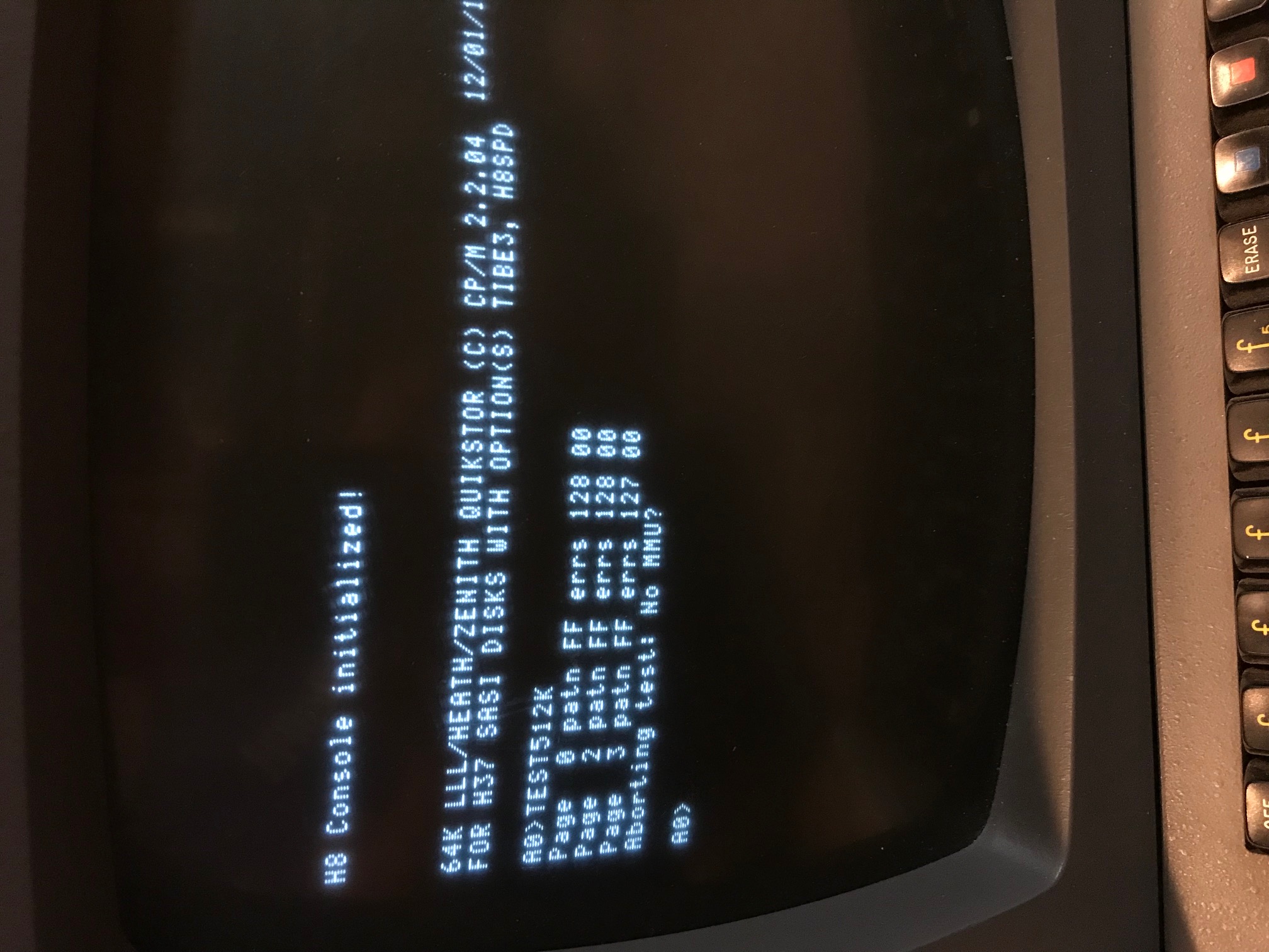
I see two issues;
1. Your TEST512K program, writes to the registers, but I do not think it is enabling Bit D7 (MAP) as I do not see activity on A16, A17, A18 on the scope. The same when booting CPM3.
2. A hardware design issue
a. On power-on or reset port 000Q glitches and the MAP signal goes high and system fails to INIT properly. It is very hard to reset the system properly. Investigating issue!
Pictures attached!
Thanks,
Norberto
To view this discussion on the web visit https://groups.google.com/d/msgid/sebhc/BF800708-B568-40FC-9317-C6362B15900C%40koyado.com.
Douglas Miller
Yes, the port address is 000Q, I'm guessing you answered that
yourself already.
The code should be setting the MAP bit, I reviewed it and it does that. Also, the simulator would have prevented it from working unless it sets MAP.
I'm not seeing what could glitch during RESET, but maybe some
conditions after RESET are causing a problem. /RESET is directly
tied to the CLR pin on the fli-flop. The only thing I can think of
is the port is getting strobed unexpectedly. I assumed the H8 bus
signal I/OW is prevented from going active during Z80 interrupt
acknowledge? Since /WR from the Z80 should never be active then, I
can't see how it could malfunction. Can you confirm whether MAP is
set when the CPU comes out of reset - as opposed to a short time
after?
To view this discussion on the web visit https://groups.google.com/d/msgid/sebhc/CB84E423-6540-4639-9854-6B45F01CF3EE%40koyado.com.
Douglas Miller
Oh, I mis-read my own test output... We don't know the
miscompared data, only the count and initial offset. So, in all
cases the buffer seems to miscompare on all (or nearly all) bytes
starting at offset 00.
The test program initially sets up a pattern buffer at 4000H (segment 1) using the BCD seed 99 (this seed is never used again). This is done before MAP is set. Then, it maps page 0 into segment 1 (leaving page 0 still mapped at segment 0, also) and then compares 0000H to 4000H. It then does the same mapping pages 1 (4000H), 2 (8000H), and 3 (C000H) into segment 1 (obviously, mapping page 1 to segment 1 is a no-op - but it does confirm correct operation).
If all the above succeeds (it does not in our case), then the
program tests each page 4-31 by first mapping each page into
segment 1 and writing a BCD pattern using a different seed, then
going back through each page 4-31 and confirming that the expected
pattern still exists. Again, we never reach this stage of the
test.
I'm guessing that basic memory operation must be working (MAP
off), otherwise you couldn't boot Heath CP/M and start the memory
test. And, the fact that the initial pattern is written to 4000H
before MAP is set probably indicates that it succeeded (you should
see that BCD pattern at 4000H-407FH). Additionally, the program is
still able to run after MAP is enabled, so that seems to indicate
that MAP does not totally break things. We see the expected
behavior of page 1 passing, but all other pages 0, 2, and 3 fail
in every byte (or at least all but one). I am guessing that the
mapping is not working at all - either MAP never actually gets set
or else writing to the MMU registers fails. My first guess would
be that the MMU is never getting out of the pass-though (default
power on) state.
To view this discussion on the web visit https://groups.google.com/d/msgid/sebhc/d84e73a2-4fed-1a37-e223-61960ad91577%40gmail.com.
Norberto Collado
By forcing MAP off via the jumper, it works fine on power-on and/or reset. The /reset line is fine, and there is a glitch on the I/OW signal at power-on or reset. I think the easy way will be to extend the reset line to stay low longer than expected to keep the MAP low until the CPU completes all its tasks. Or add a couple of 74LS14 in series to clean up the spike on the output of the I/O decoder or add a 74LS123 or 555 to eliminate such glitch.
The main issue right now is for the TEST512K test to pass. Can you create another version of TEST512K to loop so that I can check with the scope the circuit? Perhaps something like TEST512L.COM.
To view this discussion on the web visit https://groups.google.com/d/msgid/sebhc/41fd4f97-b42f-fb78-bffd-0f7017f4cb77%40gmail.com.
Norberto Collado
No need to write the TEST512L.COM program. I think I found the problem.
To view this discussion on the web visit https://groups.google.com/d/msgid/sebhc/8C4B3C70-9BEB-4ECA-A686-3A6B1BD7E645%40koyado.com.
Norberto Collado
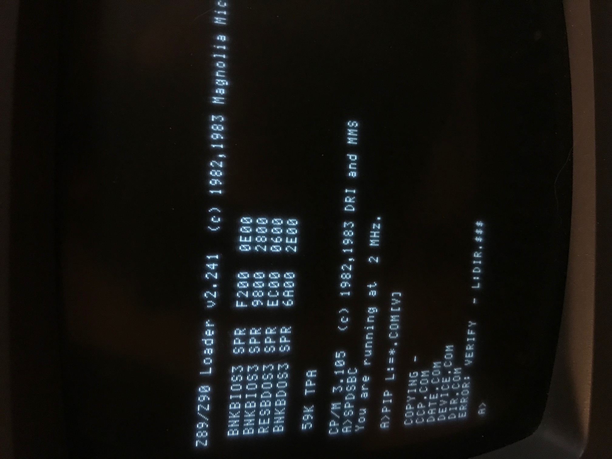
Douglas,
I found an error and corrected it. Now the memory test passes and I was able to boot CP/M3 without any issues. You did a great job on the driver and schematics and thank you! Pictures attached.
Next step is to clean up the power-on/reset /IOW glitch issue at port 000Q.
Also, how I can use the RAMDISK as I’m not that familiar with it?
To view this discussion on the web visit https://groups.google.com/d/msgid/sebhc/41fd4f97-b42f-fb78-bffd-0f7017f4cb77%40gmail.com.
Douglas Miller
Good news. I would like to hear more about what is causing the
/IOW glitch, if you know. I'm wondering why other hardware does
not see it - is it because of this port being 000Q? Or the
critical nature of accidentally writing garbage during the glitch
(i.e. MAP=1)?
The ramdisk should just be like any other drive. The command
DRIVES.COM should tell which it is... I think I set it to L: in
that image? The driver checks the contents of the first directory
entry on boot, and if it matches the expected directory label then
it leaves the contents in-tact (it assumes the previous contents
is OK). Otherwise, it initializes a new directory label and erases
all directory entries. You can copy files to it, and set it as one
of the drives to look for commands in. Or whatever one might
choose to use it for. It is only 300K so it's not huge, but could
be used as a temporary drive (e.g. for faster compiling) or other
fast-storage space. Although, I'm not sure just how much faster it
is than Z67IDE. It certainly would be faster than floppy.
To view this discussion on the web visit https://groups.google.com/d/msgid/sebhc/D1C32E42-18C2-4575-9F10-779B9A21FF9F%40koyado.com.
Norberto Collado
There is another random issue on system reset or power-on. When the MAP is disabled by using the jumper, the memory sometimes doesn’t work. I took out all the IC’s except for the ones needed to run the memory and system is not stable. Your design is fine, but there is something else going as PAM-37 cannot copy itself to RAM. If I cannot initialize the RAM with the minimum components on power-on or reset, then there is something else going on with the board layout.
To view this discussion on the web visit https://groups.google.com/d/msgid/sebhc/50fd1f5b-9273-dd9b-e002-220e4d5e94ed%40gmail.com.
Douglas Miller
I had an awful thought this morning. The databus buffers out of
the H8-512K board are unconditionally enabled by MEMR. Is Z80
board driving this signal active even if the internal ROM is being
selected? I don't see that detail on the CPU board, so can't tell.
I'm wondering if we're getting bus contention when the ROM is
enabled.
To view this discussion on the web visit https://groups.google.com/d/msgid/sebhc/7940D412-85EA-4343-853B-7B1C840ED593%40koyado.com.
Norby
To view this discussion on the web visit https://groups.google.com/d/msgid/sebhc/498eb139-14d6-c49c-c7a0-d8d8ff5f39ee%40gmail.com.
Norberto Collado
Per spec, /ROMEN should block any external reads to the H8 bus when not asserted, excepts for writes. That means that there is a design flaw on the new Z80 CPU. To verify such, I will retest with the Trionyx CPU board.
Good observation.
Thanks,
Norberto

To view this discussion on the web visit https://groups.google.com/d/msgid/sebhc/C316737A-953F-47CC-AF25-020574FDA80E%40koyado.com.
Norberto Collado
The CPU is fine, must be timing issue with the RAM. It also fails with the Trionyx CPU. Please update the port to use 120Q instead of 000Q as 000Q glitches during power-on or reset. I cannot get the board to fail at 120Q during power-on or reset.
To view this discussion on the web visit https://groups.google.com/d/msgid/sebhc/DA81F0D6-509A-4EB5-9250-0BFD6C55C20D%40koyado.com.
Douglas Miller
I updated the Z67+Z37 image at http://sebhc.durgadas.com/mms89/images/cpm3-512k-z37-rtc-rd.z67ide.xz for the MMU port 120Q. Hope that helps. I'll build the +Z17 version later.
Let me know what else you need.
To view this discussion on the web visit https://groups.google.com/d/msgid/sebhc/14726E55-F1B8-4337-BDAD-CA02D73BCCCC%40koyado.com.
Norberto Collado
Thanks!
To view this discussion on the web visit https://groups.google.com/d/msgid/sebhc/506a26a7-df19-98cd-69ad-05b4b569d10d%40gmail.com.
Norberto Collado
That worked! Also update the TEST512K.COM program.
To view this discussion on the web visit https://groups.google.com/d/msgid/sebhc/62DC138F-6D81-41E7-8852-1AF162421899%40koyado.com.
Norberto Collado
Attached is a movie copying files from drive A: to drive L: with verify on @2MHz. I compared this design with my H8 8080A/Z80 memory controller and implemented same timing and module started to work great during power-on.
Still more to test to ensure stability.
To view this discussion on the web visit https://groups.google.com/d/msgid/sebhc/A33D8F30-B396-4085-A541-3B1EA7FEBA70%40koyado.com.

Glenn Roberts
Blinkenlights! Always fun to watch a computer “think!”, and festive too!… great work guys!
- Your TEST512K program, writes to the registers, but I do not think it is enabling Bit D7 (MAP) as I do not see activity on A16, A17, A18 on the scope. The same when booting CPM3.
- A hardware design issue
To view this discussion on the web visit https://groups.google.com/d/msgid/sebhc/0BB5AE1B-AFCE-4B10-B8BD-5BB780D3FD71%40koyado.com.

George Farris
George
> > > > > > > > > .
> > > > > > > > > https://groups.google.com/d/optout.
> > > > > > > >
> > > > > > > > --
> > > > > > > > You received this message because you are subscribed to
> > > > > > > > the Google Groups "SEBHC" group.
> > > > > > > > To unsubscribe from this group and stop receiving
> > > > > > > > emails from it, send an email to
> > > > > > > > sebhc+un...@googlegroups.com.
> > > > > > > > To post to this group, send email to
> > > > > > > > se...@googlegroups.com.
> > > > > > > > To view this discussion on the web visit
> > > > > > > > .
> > > > > > > > https://groups.google.com/d/optout.
> > > > > > >
> > > > > > > --
> > > > > > > You received this message because you are subscribed to
> > > > > > > the Google Groups "SEBHC" group.
> > > > > > > To unsubscribe from this group and stop receiving emails
> > > > > > > from it, send an email to
> > > > > > > sebhc+un...@googlegroups.com.
> > > > > > > To post to this group, send email to
> > > > > > > se...@googlegroups.com.
> > > > > > > To view this discussion on the web visit
> > > > > > > .
> > > > > > > https://groups.google.com/d/optout.
> > > > > > >
> > > > > > >
> > > > > > >
> > > > > > >
> > > > > > >
> > > > > > >
> > > > > > >
> > > > > > >
> > > > > > >
> > > > > > > --
> > > > > > > You received this message because you are subscribed to
> > > > > > > the Google Groups "SEBHC" group.
> > > > > > > To unsubscribe from this group and stop receiving emails
> > > > > > > from it, send an email to
> > > > > > > sebhc+un...@googlegroups.com.
> > > > > > > To post to this group, send email to
> > > > > > > se...@googlegroups.com.
> > > > > > > To view this discussion on the web visit
> > > > > > > .
> > > > > > > https://groups.google.com/d/optout.
> > > > > > >
> > > > > > >
> > > > > > >
> > > > > > >
> > > > > > >
> > > > > > >
> > > > > > >
> > > > > > >
> > > > > > > --
> > > > > > > You received this message because you are subscribed to
> > > > > > > the Google Groups "SEBHC" group.
> > > > > > > To unsubscribe from this group and stop receiving emails
> > > > > > > from it, send an email to
> > > > > > > sebhc+un...@googlegroups.com.
> > > > > > > To post to this group, send email to
> > > > > > > se...@googlegroups.com.
> > > > > > > To view this discussion on the web visit
> > > > > > > .
> > > > > > > https://groups.google.com/d/optout.
> > > > > >
> > > > > > --
> > > > > > You received this message because you are subscribed to the
> > > > > > Google Groups "SEBHC" group.
> > > > > > To unsubscribe from this group and stop receiving emails
> > > > > > from it, send an email to
> > > > > > sebhc+un...@googlegroups.com.
> > > > > > To post to this group, send email to se...@googlegroups.com
> > > > > > .
> > > > > > .
> > > > >
> > > > > --
> > > > > You received this message because you are subscribed to the
> > > > > Google Groups "SEBHC" group.
> > > > > To unsubscribe from this group and stop receiving emails from
> > > > > it, send an email to sebhc+un...@googlegroups.com.
> > > > > To post to this group, send email to se...@googlegroups.com.
> > > > > To view this discussion on the web visit
> > > > > .
> > > > >
> > > > >
> > > > >
> > > > >
> > > > >
> > > > >
> > > > >
> > > > > --
> > > > > You received this message because you are subscribed to the
> > > > > Google Groups "SEBHC" group.
> > > > > To unsubscribe from this group and stop receiving emails from
> > > > > it, send an email to sebhc+un...@googlegroups.com.
> > > > > To post to this group, send email to se...@googlegroups.com.
> > > > > To view this discussion on the web visit
> > > > > .
> > > >
> > > > --
> > > > You received this message because you are subscribed to the
> > > > Google Groups "SEBHC" group.
> > > > To unsubscribe from this group and stop receiving emails from
> > > > it, send an email to sebhc+un...@googlegroups.com.
> > > > To post to this group, send email to se...@googlegroups.com.
> > > > To view this discussion on the web visit
> > > > .
> > > >
> > > >
> > > >
> > > >
> > > >
> > > >
> > > > --
> > > > You received this message because you are subscribed to the
> > > > Google Groups "SEBHC" group.
> > > > To unsubscribe from this group and stop receiving emails from
> > > > it, send an email to sebhc+un...@googlegroups.com.
> > > > To post to this group, send email to se...@googlegroups.com.
> > > > To view this discussion on the web visit
> > > > .
> > >
> > > --
> > > You received this message because you are subscribed to the
> > > Google Groups "SEBHC" group.
> > > To unsubscribe from this group and stop receiving emails from it,
> > > send an email to sebhc+un...@googlegroups.com.
> > > To post to this group, send email to se...@googlegroups.com.
> > > To view this discussion on the web visit
> > > .
> >
> > --
> > You received this message because you are subscribed to the Google
> > Groups "SEBHC" group.
> > To unsubscribe from this group and stop receiving emails from it,
> > send an email to sebhc+un...@googlegroups.com.
> > To post to this group, send email to se...@googlegroups.com.
> > To view this discussion on the web visit
> > .
> >
> >
> >
> >
> >
> > --
> > You received this message because you are subscribed to the Google
> > Groups "SEBHC" group.
> > To unsubscribe from this group and stop receiving emails from it,
> > send an email to sebhc+un...@googlegroups.com.
> > To post to this group, send email to se...@googlegroups.com.
> > To view this discussion on the web visit
> > .
> >
> >
> >
> >
> > --
> > You received this message because you are subscribed to the Google
> > Groups "SEBHC" group.
> > To unsubscribe from this group and stop receiving emails from it,
> > send an email to sebhc+un...@googlegroups.com.
> > To post to this group, send email to se...@googlegroups.com.
> > To view this discussion on the web visit
> > .
>
> --
> You received this message because you are subscribed to the Google
> Groups "SEBHC" group.
> To unsubscribe from this group and stop receiving emails from it,
> send an email to sebhc+un...@googlegroups.com.
> To post to this group, send email to se...@googlegroups.com.
> To view this discussion on the web visit
> .
>
>
>
> --
> You received this message because you are subscribed to the Google
> Groups "SEBHC" group.
> To unsubscribe from this group and stop receiving emails from it,
> send an email to sebhc+un...@googlegroups.com.
> To post to this group, send email to se...@googlegroups.com.
> To view this discussion on the web visit
> .
>
>
> --
> You received this message because you are subscribed to the Google
> Groups "SEBHC" group.
> To unsubscribe from this group and stop receiving emails from it,
> send an email to sebhc+un...@googlegroups.com.
> To post to this group, send email to se...@googlegroups.com.
> To view this discussion on the web visit
> .
>
> --
> You received this message because you are subscribed to the Google
> Groups "SEBHC" group.
> To unsubscribe from this group and stop receiving emails from it,
> send an email to sebhc+un...@googlegroups.com.
> To post to this group, send email to se...@googlegroups.com.
> To view this discussion on the web visit
> .
Douglas Miller
OK, updated images, including TEST512K.COM.
http://sebhc.durgadas.com/mms89/images/
I'm curious to see what timing changes were needed - it will help
me better understand the H8.
To view this discussion on the web visit https://groups.google.com/d/msgid/sebhc/0BB5AE1B-AFCE-4B10-B8BD-5BB780D3FD71%40koyado.com.
Norberto Collado
Norberto Collado
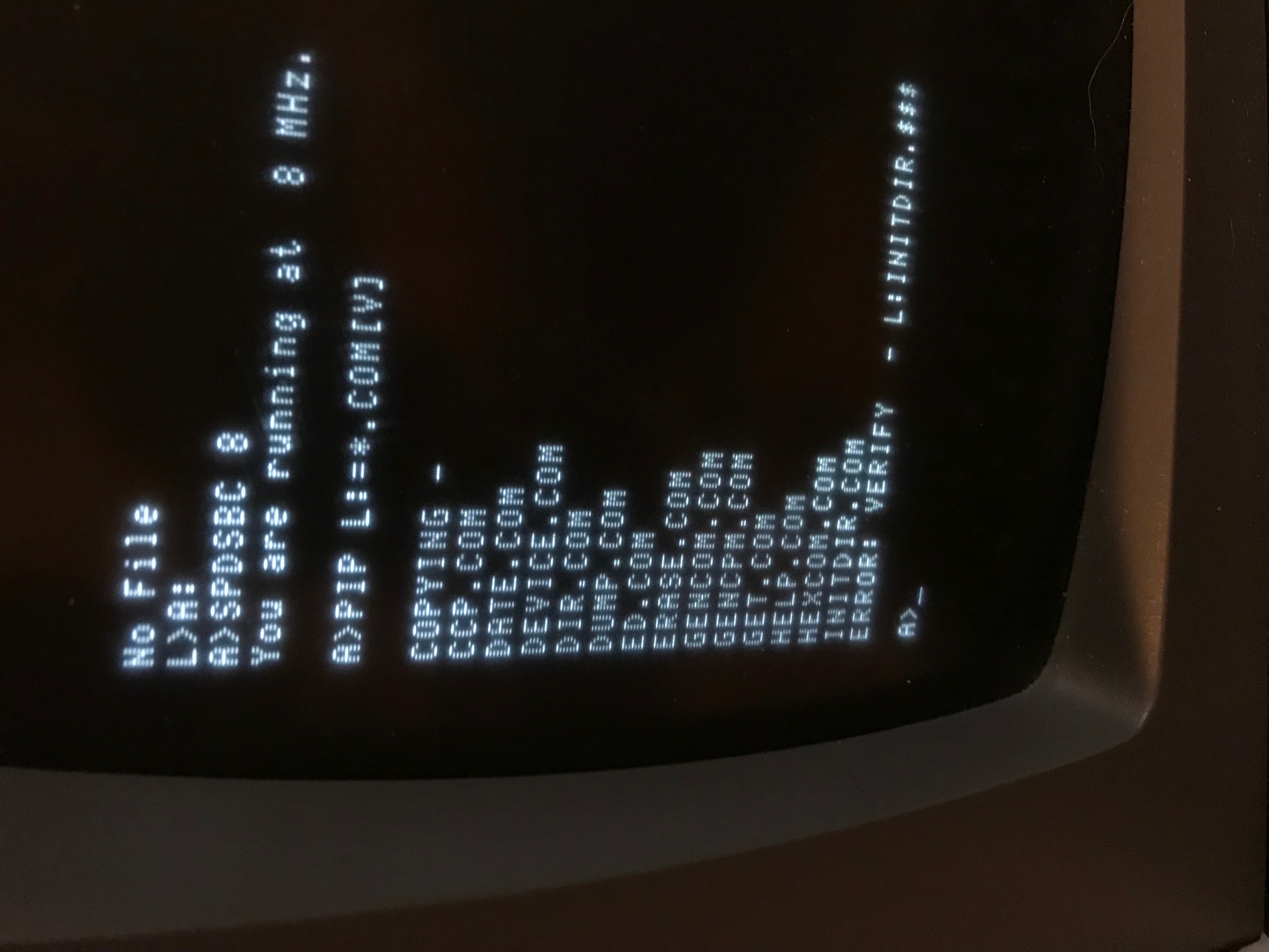
Thanks Douglas! 512Kb RAM board is now stable during power-on and on system reset, on continuous operations No new HW issues so far. Battery backup is working fine. Contents on drive L: are preserved (RAM Disk) during power failures or system resets.
There is one minor random issue when copying files from the hard drive to the RAM floppy drive. Sometimes it fails to verify the file that was copied. I did check everything and cannot see any issues so far. At 8 MHz, it copies more files than 2 MHz. Eventually I can copy A:*.com files @ 2MHz into the RAM disk.
See attached pictures.
To view this discussion on the web visit https://groups.google.com/d/msgid/sebhc/94fbca18-e26f-2044-1e4c-7e38f3e6d0d9%40gmail.com.
Douglas Miller
Ugh, that's not good. I'll have to write a more-intensive memory test, although I suspect it is going to require scope or logic analyzer traces to figure it out. I'll write a memory test that runs continuously and blips the H17 side-select bit in the control port when it sees an error. Although, the blip will be *after* the error is detected. I'll write the test to do on each byte a write-read-verify so any detected errors are reported close to the actual failure.
I'm guessing you will eventually see a crash in CP/M as well, as
I don't think this is confined to the ramdisk. Unless there is
some narrow exposure to interrupts, or the like, during the
ramdisk transfers - but I don't see that (interrupts are disabled
during the mapping and transfer).
To view this discussion on the web visit https://groups.google.com/d/msgid/sebhc/84EDE7CA-22DB-4872-B43D-B8F6AC83F01B%40koyado.com.
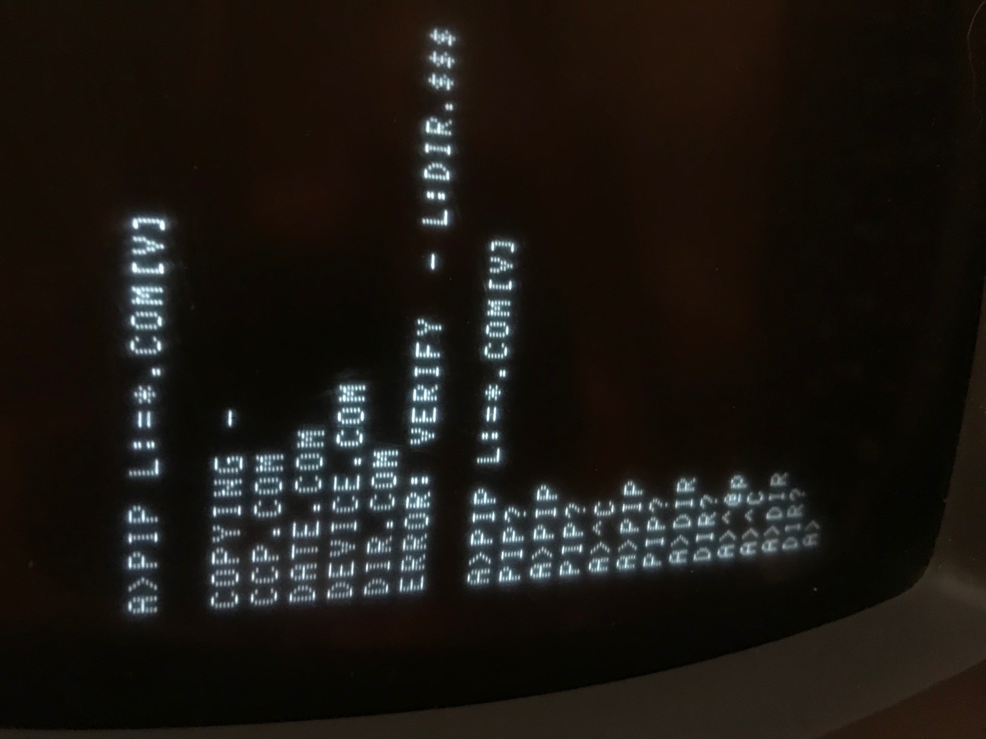
Norberto Collado
Eventually CP/M will become unstable as shown in the attached file! Other times it hangs after failure.
To view this discussion on the web visit https://groups.google.com/d/msgid/sebhc/297ec90e-4a71-6d1d-b511-48f9204d24d6%40gmail.com.
Douglas Miller
Here's a test program
http://sebhc.durgadas.com/mms89/images/strs512k.com, like TEST512K
it runs only under Heath CP/M. It's simple, but will continuously
test one page of memory, mapped into 4000H. By default it tests
page 1, you can try others by adding the page number (4-31) on the
command line. It tests silently, but will blip the H17 side select
bit every time it encounters an error. Pressing any key will end
the test and print results. The error counter pegs at 255 (won't
increase after that). It disables interrupts during the test, to
cut down on "noise". The H37 drive select will stay on because of
that.
Hopefully, you can put a scope or logic analyzer on the side select and watch for errors, or just let it run for awhile and then terminate it.
If the problem relies on some special timing, this may not find
it. If necessary, I can make the test more complicated and do
cross-page copying. But lets try this first to see if a simpler
test can find it.
To view this discussion on the web visit https://groups.google.com/d/msgid/sebhc/1B0C34D9-0DE7-44C8-8F32-F51EEA870150%40koyado.com.
Norberto Collado
I ran each page manually without any issues. Can you modify it to run all pages without the need to type the page and loop continuous thru all pages?
Thanks,
Norberto
- Your TEST512K program, writes to the registers, but I do not think it is enabling Bit D7 (MAP) as I do not see activity on A16, A17, A18 on the scope. The same when booting CPM3.
- A hardware design issue
To view this discussion on the web visit https://groups.google.com/d/msgid/sebhc/2e73418b-4384-c971-d9ba-50fc2e05a97a%40gmail.com.
Douglas Miller
I can do that, but I suspect the problem is not with one particular page but with the timing, possibly in combination with inter-bank moves. I'll see what it takes to rotate through all pages, and also start thinking about how to redesign the test for inter-bank moves, simulating the ldir timing (but still checking every byte).
Do you want the test to stop on error? Or is it fine to just
pulse the side-select pin?
To view this discussion on the web visit https://groups.google.com/d/msgid/sebhc/6ADB13DB-24A0-478F-890E-70DC27A11C4A%40koyado.com.
Douglas Miller
OK, I updated STRS512K.COM to test all pages. It does not stop on
error, but pulses side-select. It tests pages 1,4-31 as pages
0,2,3 are used by the system and I did not want to corrupt those.
To view this discussion on the web visit https://groups.google.com/d/msgid/sebhc/9e555fa9-67a2-417d-306f-081718da26db%40gmail.com.
Norberto Collado
So far running the test without any issues. The scope is set to monitor the side-select signal. I will let it run for several hrs.
To view this discussion on the web visit https://groups.google.com/d/msgid/sebhc/c6857da4-8464-08dd-f6ac-49e5e4f46bf6%40gmail.com.

Kenneth L. Owen
So far running the test without any issues. The scope is set to monitor the side-select signal. I will let it run for several hrs.
To post to this group, send email to mailto:sebhc@googlegroupscom.
To post to this group, send email to mailto:sebhc@googlegroupscom.
To view this discussion on the web visit https://groups.google.com/d/msgid/sebhc/C316737A-953F-47CC-AF25-020574FDA80E%40koyado.com.
For more options, visit https://groups.google.com/d/optout.
--
You received this message because you are subscribed to the Google Groups "SEBHC" group.
To unsubscribe from this group and stop receiving emails from it, send an email to sebhc+un...@googlegroups.com.
To post to this group, send email to se...@googlegroups.com.
To view this discussion on the web visit https://groups.google.com/d/msgid/sebhc/DA81F0D6-509A-4EB5-9250-0BFD6C55C20D%40koyado.com.
For more options, visit https://groupsgoogle.com/d/optout.
You received this message because you are subscribed to the Google Groups "SEBHC" group.
To unsubscribe from this group and stop receiving emails from it, send an email to sebhc+un...@googlegroups.com.
To post to this group, send email to se...@googlegroups.com.
Norberto Collado
Thanks Ken! So far no errors and the scope on the side select signal stills the same; no triggers. See attached movie on memory test patterns.
To view this discussion on the web visit https://groups.google.com/d/msgid/sebhc/5B842FFF1B1547F8A9C5DFBF8F763FAD%40KenPSPC.
Douglas Miller
The movie indicates the program is doing what I intended...
except not finding any errors. If it doesn't find any errors, I'll
have to redesign the test to try and match what goes on during
inter-bank copying. I may have to give up on the idea of catching
the error at exactly the byte where it occurs. I guess the first
priority should be to reproduce the error reliably.
To view this discussion on the web visit https://groups.google.com/d/msgid/sebhc/64CEC702-1534-4913-BA6F-D84F7BB9D5A5%40koyado.com.
Norberto Collado
I change the way /CS is selected and now it works at 8 MHz without any issues. The board can only be 2 slots away from the Z80 board to work properly. It should be installed behind the CPU to maintain proper throughput at 8 MHz’s.
I will do more testing until I feel that it is bullet proof. I will like the board to work at 4 slots away from the CPU if possible.
To view this discussion on the web visit https://groups.google.com/d/msgid/sebhc/ae6421c6-73bb-a49f-2e1d-8dd5c3199027%40gmail.com.
Douglas Miller
I'll be really interested to see the final schematics/changes.
I'd like to learn more about these sorts of issues.
To view this discussion on the web visit https://groups.google.com/d/msgid/sebhc/7978BFAE-AC8D-4670-B3F7-20AD9482172A%40koyado.com.
Norberto Collado
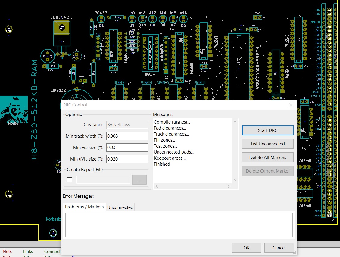
It is all about propagation delays and correct timing. The schematics WIP due to all issues encountered.
Changes to the read cycle to fix RAMDISK verify issue.
1. Change the read cycle from OE# controlled to address controlled to get more stability
2. Change CE# from address controlled to CE# controlled to get additional stability.
3. I might add a flip flop to keep the read buffers “On” longer than expected. Need to evaluate such change.
I ordered faster 74LS670’s to evaluate the timing at different slots. So far with these changes, I can run the board at 8 MHz without any issues.
To view this discussion on the web visit https://groups.google.com/d/msgid/sebhc/39952cd7-2f66-77ec-6c6b-333f84ec9ed0%40gmail.com.
Douglas Miller
I don't understand #1 and #2, perhaps I need to wait for the
schematic. If those refer to the control pins on the 512Kx8 SRAM
chip, I suspected that was not quite right. But I was also
concerned about the propagation delays through the 74LS670s. I was
wondering about the double-inversion of MEMR on it's way to the
'670s - although the READ path is only inverted once (WRITE =
!READ, so writes should not suffer).
So, you are currently not seeing any issues on the range 2MHz to
8MHz? No more crashes in CP/M3? And the STRS512K.COM program never
showed any errors?
To view this discussion on the web visit https://groups.google.com/d/msgid/sebhc/826B2C28-7C87-47BF-A7C9-BAADF663B878%40koyado.com.
Norberto Collado
To view this discussion on the web visit https://groups.google.com/d/msgid/sebhc/8c2ffa7b-4c82-2d99-0524-760a6a072397%40gmail.com.
Douglas Miller
Ah, OK, that is making sense. I see the truth-table for the SRAM
shows that OE and WE are not mutually exclusive. Does that mean
you'll need to change the enable logic on the databus buffers as
well? And also for I/O WR, to avoid conflict with the SRAM which
will be in data output mode during an I/O WR cycle? Or
split-out/isolate the I/O databus?
To view this discussion on the web visit https://groups.google.com/d/msgid/sebhc/20181226112725.1321cca37f09b4ab87c5049afdc8ceaa.045a5cee2b.wbe%40email09.godaddy.com.
Norberto Collado
To view this discussion on the web visit https://groups.google.com/d/msgid/sebhc/f9207fe8-e125-3bf5-ab29-51c80c8f6d2f%40gmail.com.
Norberto Collado
To view this discussion on the web visit https://groups.google.com/d/msgid/sebhc/20181226161854.1321cca37f09b4ab87c5049afdc8ceaa.ab9cdee137.wbe%40email09.godaddy.com.
Norberto Collado
To view this discussion on the web visit https://groups.google.com/d/msgid/sebhc/20181226163808.1321cca37f09b4ab87c5049afdc8ceaa.30a2cd2552.wbe%40email09.godaddy.com.
Douglas Miller
One thing I was wondering about, with the new output enables, was what happens when the '244 and SRAM both are driving the internal databus at the same time, even if no operations are going on. I think they both are enabled, but I'm not entirely sure what signals are being used in both cases.
I can't think of any reason that BKA18 would be active when CP/M
is at the prompt. Only the ramdisk would normally use that range
of RAM, and I can't think of any interrupt conditions that would
ever result in ramdisk being accessed. Sounds like maybe the
internal databus is not cleanly allowing output to the bank select
'670s?
To view this discussion on the web visit https://groups.google.com/d/msgid/sebhc/20181227133904.1321cca37f09b4ab87c5049afdc8ceaa.8e95536057.wbe%40email09.godaddy.com.
Norberto Collado
To view this discussion on the web visit https://groups.google.com/d/msgid/sebhc/25ce0e73-99f7-4b2e-570f-499c9b90e49a%40gmail.com.
Norberto Collado
Hello Douglas,
Added a gate to control the writes during I/OW and MEMWR and the pulse on BKA18 went away as there was data contention between the RAM IC and the write buffer after making last night changes. Thanks for pointing that out as it saved debug time. Thank you! Thank you!
After adding the gate to control the writes for memory and I/O, now I can successfully copy files to the L: drive (RAMDISK) without any issues. I have been testing it @2MHz and 8MHz for hrs without further issues.
I will keep testing it to ensure that we do not have any other issues. Right now, is running a batch job copying files from the hard drive to the RAM drive. At 8MHz is really fast.
Thanks,
Norberto
To view this discussion on the web visit https://groups.google.com/d/msgid/sebhc/20181227151814.1321cca37f09b4ab87c5049afdc8ceaa.e9df63f5ad.wbe%40email09.godaddy.com.
Douglas Miller
Great news! Hopefully the changes are not too bad. I look forward
to seeing the revised schematic, so I can learn. It's a moot
point, but I wonder if this would have worked better directly
connected to the Z80, rather than having to conform to the H8 bus.
I've wondered about the propagation delays introduced by
converting the Z80 bus controls into the H8 bus signals, and back
again. Maybe it would have been a wash.
To view this discussion on the web visit https://groups.google.com/d/msgid/sebhc/7BC41C5D-C102-464F-A0DB-01DCD6360B36%40koyado.com.
Norberto Collado
I wonder if this would have worked better directly connected to the Z80,
Yes, to this as it gives you the best performance. That is why the memory board has to be behind the CPU to avoid issues, when pushing the CPU speed beyond 2 MHz’s. Anyhow we need to make this work to support the Heath Z80 board as well. I had no issues with the X/2 solution. The system ran all night without any issues.
I will keep testing today on power-on and system reset to ensure that the system always initializes properly.
To view this discussion on the web visit https://groups.google.com/d/msgid/sebhc/76c2dd2e-f98b-e0ef-84bc-2d07a90bb5f2%40gmail.com.
Norberto Collado
Found another issue during Power-on. I have a DS1210 to protect the RAM content during power loss and during power-on it latches at random causing the RAM to go offline. So, I will eliminate it to avoid such condition. Working on an alternative. See attached movie on a power-on DS1210 latch condition.
To view this discussion on the web visit https://groups.google.com/d/msgid/sebhc/3196F1EA-A2EA-4FDA-851A-68C88491C8A7%40koyado.com.
Norberto Collado
To view this discussion on the web visit https://groups.google.com/d/msgid/sebhc/4FF34428-DD85-42C2-B066-E7BA7B07CA19%40koyado.com.
Norberto Collado
Latest schematics at the website: http://koyado.com/Heathkit/H8-512KB_RAM_MMU.html
To view this discussion on the web visit https://groups.google.com/d/msgid/sebhc/20181228225518.1321cca37f09b4ab87c5049afdc8ceaa.4b726543e0.wbe%40email09.godaddy.com.
Norberto Collado
Hello Douglas,
I put a hardware fix to filter out the port glitch issue. Can we have all the images and test applications back to used 000Q port? I’m testing with the H17 image at 00Q without any issues.
Sorry for the trash and thanks for all your support.
I think we have a working board from 2 to 8 MHz’s. I haven’t tested at 10MHz, as I need the new CPU board.
Thanks,
Norberto
From: "se...@googlegroups.com" <se...@googlegroups.com> on behalf of Douglas Miller <durga...@gmail.com>
Reply-To: "se...@googlegroups.com" <se...@googlegroups.com>
Date: Sunday, December 23, 2018 at 7:45 PM
To: "se...@googlegroups.com" <se...@googlegroups.com>
Subject: Re: [sebhc] Testing H8-512KB RAM PCB
I updated the Z67+Z37 image at http://sebhc.durgadas.com/mms89/images/cpm3-512k-z37-rtc-rd.z67ide.xz for the MMU port 120Q. Hope that helps. I'll build the +Z17 version later.
Let me know what else you need.
On 12/23/18 8:03 PM, Norberto Collado wrote:
The CPU is fine, must be timing issue with the RAM. It also fails with the Trionyx CPU. Please update the port to use 120Q instead of 000Q as 000Q glitches during power-on or reset. I cannot get the board to fail at 120Q during power-on or reset.
Thanks,
Norberto
From: "se...@googlegroups.com" <se...@googlegroups.com> on behalf of Norberto Collado <norberto...@koyado.com>
Reply-To: "se...@googlegroups.com" <se...@googlegroups.com>
Date: Sunday, December 23, 2018 at 12:57 PM
To: "se...@googlegroups.com" <se...@googlegroups.com>
Subject: Re: [sebhc] Testing H8-512KB RAM PCB
Per spec, /ROMEN should block any external reads to the H8 bus when not asserted, excepts for writes. That means that there is a design flaw on the new Z80 CPU. To verify such, I will retest with the Trionyx CPU board.
Good observation.
Thanks,
Norberto
From: "se...@googlegroups.com" <se...@googlegroups.com> on behalf of Norby <norberto...@koyado.com>
Reply-To: "se...@googlegroups.com" <se...@googlegroups.com>
Date: Sunday, December 23, 2018 at 10:20 AM
To: "se...@googlegroups.com" <se...@googlegroups.com>
Subject: Re: [sebhc] Testing H8-512KB RAM PCB
I will check it out and thanks for the feedback. When I get a good copy of Pam37 the system is very stable. If this is the case it is an easy fix.
Sent from my iPhone
On Dec 23, 2018, at 5:17 AM, Douglas Miller <durga...@gmail.com> wrote:
I had an awful thought this morning. The databus buffers out of the H8-512K board are unconditionally enabled by MEMR. Is Z80 board driving this signal active even if the internal ROM is being selected? I don't see that detail on the CPU board, so can't tell. I'm wondering if we're getting bus contention when the ROM is enabled.
On 12/22/18 6:20 PM, Norberto Collado wrote:
There is another random issue on system reset or power-on. When the MAP is disabled by using the jumper, the memory sometimes doesn’t work. I took out all the IC’s except for the ones needed to run the memory and system is not stable. Your design is fine, but there is something else going as PAM-37 cannot copy itself to RAM. If I cannot initialize the RAM with the minimum components on power-on or reset, then there is something else going on with the board layout.
Thanks,
Norberto
From: "se...@googlegroups.com" <se...@googlegroups.com> on behalf of Douglas Miller <durga...@gmail.com>
Reply-To: "se...@googlegroups.com" <se...@googlegroups.com>
Date: Saturday, December 22, 2018 at 1:05 PM
To: "se...@googlegroups.com" <se...@googlegroups.com>
Subject: Re: [sebhc] Testing H8-512KB RAM PCB
Good news. I would like to hear more about what is causing the /IOW glitch, if you know. I'm wondering why other hardware does not see it - is it because of this port being 000Q? Or the critical nature of accidentally writing garbage during the glitch (i.e. MAP=1)?
The ramdisk should just be like any other drive. The command DRIVES.COM should tell which it is... I think I set it to L: in that image? The driver checks the contents of the first directory entry on boot, and if it matches the expected directory label then it leaves the contents in-tact (it assumes the previous contents is OK). Otherwise, it initializes a new directory label and erases all directory entries. You can copy files to it, and set it as one of the drives to look for commands in. Or whatever one might choose to use it for. It is only 300K so it's not huge, but could be used as a temporary drive (e.g. for faster compiling) or other fast-storage space. Although, I'm not sure just how much faster it is than Z67IDE. It certainly would be faster than floppy.
On 12/22/18 1:49 PM, Norberto Collado wrote:
Douglas,
I found an error and corrected it. Now the memory test passes and I was able to boot CP/M3 without any issues. You did a great job on the driver and schematics and thank you! Pictures attached.
Next step is to clean up the power-on/reset /IOW glitch issue at port 000Q.
Also, how I can use the RAMDISK as I’m not that familiar with it?
Thanks,
Norberto
From: "se...@googlegroups.com" <se...@googlegroups.com> on behalf of Douglas Miller <durga...@gmail.com>
Reply-To: "se...@googlegroups.com" <se...@googlegroups.com>
Date: Saturday, December 22, 2018 at 7:20 AM
To: "se...@googlegroups.com" <se...@googlegroups.com>
Subject: Re: [sebhc] Testing H8-512KB RAM PCB
Oh, I mis-read my own test output... We don't know the miscompared data, only the count and initial offset. So, in all cases the buffer seems to miscompare on all (or nearly all) bytes starting at offset 00.
The test program initially sets up a pattern buffer at 4000H (segment 1) using the BCD seed 99 (this seed is never used again). This is done before MAP is set. Then, it maps page 0 into segment 1 (leaving page 0 still mapped at segment 0, also) and then compares 0000H to 4000H. It then does the same mapping pages 1 (4000H), 2 (8000H), and 3 (C000H) into segment 1 (obviously, mapping page 1 to segment 1 is a no-op - but it does confirm correct operation).
If all the above succeeds (it does not in our case), then the program tests each page 4-31 by first mapping each page into segment 1 and writing a BCD pattern using a different seed, then going back through each page 4-31 and confirming that the expected pattern still exists. Again, we never reach this stage of the test.
I'm guessing that basic memory operation must be working (MAP off), otherwise you couldn't boot Heath CP/M and start the memory test. And, the fact that the initial pattern is written to 4000H before MAP is set probably indicates that it succeeded (you should see that BCD pattern at 4000H-407FH). Additionally, the program is still able to run after MAP is enabled, so that seems to indicate that MAP does not totally break things. We see the expected behavior of page 1 passing, but all other pages 0, 2, and 3 fail in every byte (or at least all but one). I am guessing that the mapping is not working at all - either MAP never actually gets set or else writing to the MMU registers fails. My first guess would be that the MMU is never getting out of the pass-though (default power on) state.
On 12/22/18 8:03 AM, Douglas Miller wrote:
Yes, the port address is 000Q, I'm guessing you answered that yourself already.
The code should be setting the MAP bit, I reviewed it and it does that. Also, the simulator would have prevented it from working unless it sets MAP.
I'm not seeing what could glitch during RESET, but maybe some conditions after RESET are causing a problem. /RESET is directly tied to the CLR pin on the fli-flop. The only thing I can think of is the port is getting strobed unexpectedly. I assumed the H8 bus signal I/OW is prevented from going active during Z80 interrupt acknowledge? Since /WR from the Z80 should never be active then, I can't see how it could malfunction. Can you confirm whether MAP is set when the CPU comes out of reset - as opposed to a short time after?
The output from TEST512K suggests that it read FF on the first miscompared byte. I know you'd get fields of alternating FF and 00 in old DRAM on power up - but this is modern SRAM. Does the FF indicate that the SRAM is not getting enabled? I don't see how that could be failing and the system could run at all, though.
I'll keep staring at the schematic, but any more detail you can collect will help.
P.S. it looks like TEST512K is failing before it tests the extended memory (pages 4-31), so you probably won't see any activity on A16-18 - until such time as it is able to pass the first 4 pages test. Otherwise, it would crash miserably in situations like this, which would be nice to avoid.
On 12/22/18 2:09 AM, Norberto Collado wrote:
Hello Douglas,
I see two issues;
1. Your TEST512K program, writes to the registers, but I do not think it is enabling Bit D7 (MAP) as I do not see activity on A16, A17, A18 on the scope. The same when booting CPM3.
2. A hardware design issue
a. On power-on or reset port 000Q glitches and the MAP signal goes high and system fails to INIT properly. It is very hard to reset the system properly. Investigating issue!
Pictures attached!
Thanks,
Norberto
From: "se...@googlegroups.com" <se...@googlegroups.com> on behalf of Norberto Collado <norberto...@koyado.com>
Reply-To: "se...@googlegroups.com" <se...@googlegroups.com>
Date: Friday, December 21, 2018 at 10:24 PM
To: "se...@googlegroups.com" <se...@googlegroups.com>
Subject: Re: [sebhc] H8-512KB of RAM
Hello Douglas,
What is the port address for the 512K board? 000Q or ??? For the Test512k program to work.
Thanks,
Norberto
To post to this group, send email to se...@googlegroups.com.
To view this discussion on the web visit https://groups.google.com/d/msgid/sebhc/C316737A-953F-47CC-AF25-020574FDA80E%40koyado.com.
For more options, visit https://groups.google.com/d/optout.
--
You received this message because you are subscribed to the Google Groups "SEBHC" group.
To unsubscribe from this group and stop receiving emails from it, send an email to sebhc+un...@googlegroups.com.
To post to this group, send email to se...@googlegroups.com.
To view this discussion on the web visit https://groups.google.com/d/msgid/sebhc/DA81F0D6-509A-4EB5-9250-0BFD6C55C20D%40koyado.com.
For more options, visit https://groups.google.com/d/optout.
--
You received this message because you are subscribed to the Google Groups "SEBHC" group.
To unsubscribe from this group and stop receiving emails from it, send an email to sebhc+un...@googlegroups.com.
To post to this group, send email to se...@googlegroups.com.
To view this discussion on the web visit https://groups.google.com/d/msgid/sebhc/14726E55-F1B8-4337-BDAD-CA02D73BCCCC%40koyado.com.
For more options, visit https://groups.google.com/d/optout.
Douglas Miller
OK! I've updated the images at http://sebhc.durgadas.com/mms89/images/ to use MMU port 0 now.
Good news. Let me know how it goes.
To view this discussion on the web visit https://groups.google.com/d/msgid/sebhc/CF02BE2E-1DBA-4A35-BAAA-4A2001755A7D%40koyado.com.
Norberto Collado
Thanks Douglas!
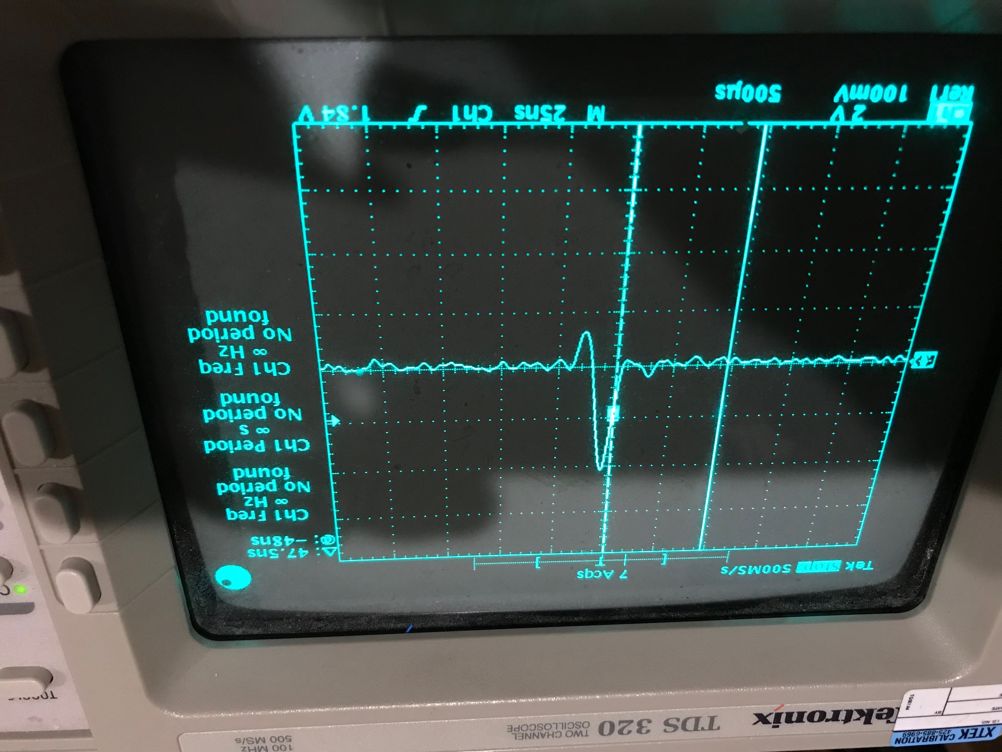
One more thing, I need you to check for me on the values loaded into the 74LS670 IC’s for A16, A17, and A18. When I boot CP/M3 to the prompt and while sitting at the prompt I see the following pulse only on A16, A17, A18 (about 1.84 volts). A14 and A15 are fine. It seems that maybe is trying to go tristate (high) for some reason. When I write at L: drive is gets larger as shown at the attached picture (~4 volts).
Any idea on why such glitch?
Thanks,
Norberto
- Your TEST512K program, writes to the registers, but I do not think it is enabling Bit D7 (MAP) as I do not see activity on A16, A17, A18 on the scope. The same when booting CPM3.
- A hardware design issue
To view this discussion on the web visit https://groups.google.com/d/msgid/sebhc/a5793dd0-7fc1-64c3-f9f6-25c844bc5894%40gmail.com.
Douglas Miller
I'm not sure if I'm reading the scope correctly, is that spike
width somewhere around 8-12 nS? One thing I can think of that the
MEMR signal is used to switch between the RD and WR pairs of 74LS670's,
and there is a one-gate delay between them due to the inverter.
So there is probably a small sliver of time where neither set of
74LS670's
are selected. That should be innocuous - I think.
Those Schmitt trigger gates do tend to be slower than the regular ones, as I recall (the schematic says 74HC14). I suspect if it were a 74'04 it would be a lot smaller spike. But, not sure why the amplitude would vary.
To view this discussion on the web visit https://groups.google.com/d/msgid/sebhc/F29926D4-F659-40FE-85A2-9471617FE3B7%40koyado.com.
Norberto Collado
-------- Original Message --------
Subject: Re: [sebhc] Testing H8-512KB RAM PCB
From: Douglas Miller <durga...@gmail.com>
To view this discussion on the web visit https://groups.google.com/d/msgid/sebhc/7a2de0f1-b914-07e7-bcfd-cdeb4ea1d664%40gmail.com.

Joseph E McGlone
George Farris
Cheers
George
> > > > > > > > > > > > .
> > > > > > > > > > > > https://groups.google.com/d/optout.
> > > > > > > > > > >
> > > > > > > > > > > --
> > > > > > > > > > > You received this message because you are
> > > > > > > > > > > subscribed to the Google Groups "SEBHC" group.
> > > > > > > > > > > To unsubscribe from this group and stop receiving
> > > > > > > > > > > emails from it, send an email to
> > > > > > > > > > > sebhc+un...@googlegroups.com.
> > > > > > > > > > > To post to this group, send email to
> > > > > > > > > > > se...@googlegroups.com.
> > > > > > > > > > > To view this discussion on the web visit
> > > > > > > > > > > .
> > > > > > > > > > > https://groups.google.com/d/optout.
> > > > > > > > > >
> > > > > > > > > > --
> > > > > > > > > > You received this message because you are
> > > > > > > > > > subscribed to the Google Groups "SEBHC" group.
> > > > > > > > > > To unsubscribe from this group and stop receiving
> > > > > > > > > > emails from it, send an email to
> > > > > > > > > > sebhc+un...@googlegroups.com.
> > > > > > > > > > To post to this group, send email to
> > > > > > > > > > se...@googlegroups.com.
> > > > > > > > > > To view this discussion on the web visit
> > > > > > > > > > .
> > > > > > > > > > https://groups.google.com/d/optout.
> > > > > > > > > >
> > > > > > > > > >
> > > > > > > > > >
> > > > > > > > > >
> > > > > > > > > >
> > > > > > > > > >
> > > > > > > > > >
> > > > > > > > > >
> > > > > > > > > > --
> > > > > > > > > > You received this message because you are
> > > > > > > > > > subscribed to the Google Groups "SEBHC" group.
> > > > > > > > > > To unsubscribe from this group and stop receiving
> > > > > > > > > > emails from it, send an email to
> > > > > > > > > > sebhc+un...@googlegroups.com.
> > > > > > > > > > To post to this group, send email to
> > > > > > > > > > se...@googlegroups.com.
> > > > > > > > > > To view this discussion on the web visit
> > > > > > > > > > .
> > > > > > > > > > https://groups.google.com/d/optout.
> > > > > > > > > >
> > > > > > > > > >
> > > > > > > > > >
> > > > > > > > > >
> > > > > > > > > >
> > > > > > > > > >
> > > > > > > > > >
> > > > > > > > > > --
> > > > > > > > > > You received this message because you are
> > > > > > > > > > subscribed to the Google Groups "SEBHC" group.
> > > > > > > > > > To unsubscribe from this group and stop receiving
> > > > > > > > > > emails from it, send an email to
> > > > > > > > > > sebhc+un...@googlegroups.com.
> > > > > > > > > > To post to this group, send email to
> > > > > > > > > > se...@googlegroups.com.
> > > > > > > > > > To view this discussion on the web visit
> > > > > > > > > > .
> > > > > > > > > > https://groups.google.com/d/optout.
> > > > > > > > >
> > > > > > > > > --
> > > > > > > > > You received this message because you are subscribed
> > > > > > > > > to the Google Groups "SEBHC" group.
> > > > > > > > > To unsubscribe from this group and stop receiving
> > > > > > > > > emails from it, send an email to
> > > > > > > > > sebhc+un...@googlegroups.com.
> > > > > > > > > To post to this group, send email to
> > > > > > > > > se...@googlegroups.com.
> > > > > > > > > To view this discussion on the web visit
> > > > > > > > > .
> > > > > > > > > https://groups.google.com/d/optout.
> > > > > > > >
> > > > > > > > --
> > > > > > > > You received this message because you are subscribed to
> > > > > > > > the Google Groups "SEBHC" group.
> > > > > > > > To unsubscribe from this group and stop receiving
> > > > > > > > emails from it, send an email to
> > > > > > > > sebhc+un...@googlegroups.com.
> > > > > > > > To post to this group, send email to
> > > > > > > > se...@googlegroups.com.
> > > > > > > > To view this discussion on the web visit
> > > > > > > > .
> > > > > > > > https://groups.google.com/d/optout.
> > > > > > > >
> > > > > > > >
> > > > > > > >
> > > > > > > >
> > > > > > > >
> > > > > > > >
> > > > > > > > --
> > > > > > > > You received this message because you are subscribed to
> > > > > > > > the Google Groups "SEBHC" group.
> > > > > > > > To unsubscribe from this group and stop receiving
> > > > > > > > emails from it, send an email to
> > > > > > > > sebhc+un...@googlegroups.com.
> > > > > > > > To post to this group, send email to
> > > > > > > > se...@googlegroups.com.
> > > > > > > > To view this discussion on the web visit
> > > > > > > > .
> > > > > > > > https://groups.google.com/d/optout.
> > > > > > >
> > > > > > > --
> > > > > > > You received this message because you are subscribed to
> > > > > > > the Google Groups "SEBHC" group.
> > > > > > > To unsubscribe from this group and stop receiving emails
> > > > > > > from it, send an email to
> > > > > > > sebhc+un...@googlegroups.com.
> > > > > > > To post to this group, send email to
> > > > > > > se...@googlegroups.com.
> > > > > > > To view this discussion on the web visit
> > > > > > > .
> > > > > > > https://groups.google.com/d/optout.
> > > > > > >
> > > > > > >
> > > > > > >
> > > > > > >
> > > > > > >
> > > > > > > --
> > > > > > > You received this message because you are subscribed to
> > > > > > > the Google Groups "SEBHC" group.
> > > > > > > To unsubscribe from this group and stop receiving emails
> > > > > > > from it, send an email to
> > > > > > > sebhc+un...@googlegroups.com.
> > > > > > > To post to this group, send email to
> > > > > > > se...@googlegroups.com.
> > > > > > > To view this discussion on the web visit
> > > > > > > .
> > > > > > > https://groups.google.com/d/optout.
> > > > > >
> > > > > > --
> > > > > > You received this message because you are subscribed to the
> > > > > > Google Groups "SEBHC" group.
> > > > > > To unsubscribe from this group and stop receiving emails
> > > > > > from it, send an email to
> > > > > > sebhc+un...@googlegroups.com.
> > > > > > To post to this group, send email to se...@googlegroups.com
> > > > > > .
> > > > > > .
> > > > >
> > > > > --
> > > > > You received this message because you are subscribed to the
> > > > > Google Groups "SEBHC" group.
> > > > > To unsubscribe from this group and stop receiving emails from
> > > > > it, send an email to sebhc+un...@googlegroups.com.
> > > > > To post to this group, send email to se...@googlegroups.com.
> > > > > To view this discussion on the web visit
> > > > > .
> > > > >
> > > > >
> > > > >
> > > > >
> > > > > --
> > > > > You received this message because you are subscribed to the
> > > > > Google Groups "SEBHC" group.
> > > > > To unsubscribe from this group and stop receiving emails from
> > > > > it, send an email to sebhc+un...@googlegroups.com.
> > > > > To post to this group, send email to se...@googlegroups.com.
> > > > > To view this discussion on the web visit
> > > > > .
> > > > >
> > > > >
> > > > >
> > > > > --
> > > > > You received this message because you are subscribed to the
> > > > > Google Groups "SEBHC" group.
> > > > > To unsubscribe from this group and stop receiving emails from
> > > > > it, send an email to sebhc+un...@googlegroups.com.
> > > > > To post to this group, send email to se...@googlegroups.com.
> > > > > To view this discussion on the web visit
> > > > > .
> > > >
> > > > --
> > > > You received this message because you are subscribed to the
> > > > Google Groups "SEBHC" group.
> > > > To unsubscribe from this group and stop receiving emails from
> > > > it, send an email to sebhc+un...@googlegroups.com.
> > > > To post to this group, send email to se...@googlegroups.com.
> > > > To view this discussion on the web visit
> > > > .
> > > >
> > > >
> > > > --
> > > > You received this message because you are subscribed to the
> > > > Google Groups "SEBHC" group.
> > > > To unsubscribe from this group and stop receiving emails from
> > > > it, send an email to sebhc+un...@googlegroups.com.
> > > > To post to this group, send email to se...@googlegroups.com.
> > > > To view this discussion on the web visit
> > > > .
> > >
> > > --
> > > You received this message because you are subscribed to the
> > > Google Groups "SEBHC" group.
> > > To unsubscribe from this group and stop receiving emails from it,
> > > send an email to sebhc+un...@googlegroups.com.
> > > To post to this group, send email to se...@googlegroups.com.
> > > To view this discussion on the web visit
> > > .
> >
> > --
> > You received this message because you are subscribed to the Google
> > Groups "SEBHC" group.
> > To unsubscribe from this group and stop receiving emails from it,
> > send an email to sebhc+un...@googlegroups.com.
> > To post to this group, send email to se...@googlegroups.com.
> > To view this discussion on the web visit
> > .
>
> --
> You received this message because you are subscribed to the Google
> Groups "SEBHC" group.
> To unsubscribe from this group and stop receiving emails from it,
> send an email to sebhc+un...@googlegroups.com.
> To post to this group, send email to se...@googlegroups.com.
> To view this discussion on the web visit
> .
Norberto Collado
To view this discussion on the web visit https://groups.google.com/d/msgid/sebhc/92398b5ea77cd75d616bb5cefbcc8816a36b6fc4.camel%40gmail.com.
Norberto Collado
I finalized today last minute changes and ordered the 512KB boards as a companion for the new/updated Z80 board.
Thanks,
Norby
To view this discussion on the web visit https://groups.google.com/d/msgid/sebhc/20181228225518.1321cca37f09b4ab87c5049afdc8ceaa.4b726543e0.wbe%40email09.godaddy.com.
Norberto Collado
Status:
I just got confirmation that the 512KB-RAM boards shipped today. I will put one together this weekend and if everything checks out, then I can start the invoices for the international orders and domestic for this board as well.
This is a good companion board for the new Z80 board to be able to run CP/M3 on the H8 systems and never seen before thanks to Douglas for his dedication/passion in supporting this idea. It is a complex/small Z80 MMU design but reliable. Also support the standard Heath CP/M/HDOS OS’s. It only works with the Z80 and not for the 8080A configuration.
A lot of testing and power cycling to get here, but I need to ensure that we have a reliable board design.
Also thanks to Gary Kaufman that provided 20-pcs of the DS1210 IC’s free of charge to support the battery backup when the board is powered down; essential to keep Drive L: alive. I will ship one for each board and also such part can be purchased from Unicorn Electronics which has them for $3.99 each.
To view this discussion on the web visit https://groups.google.com/d/msgid/sebhc/4371BF59-EBE5-467A-BBBC-F344CF54BBF6%40koyado.com.
Norberto Collado
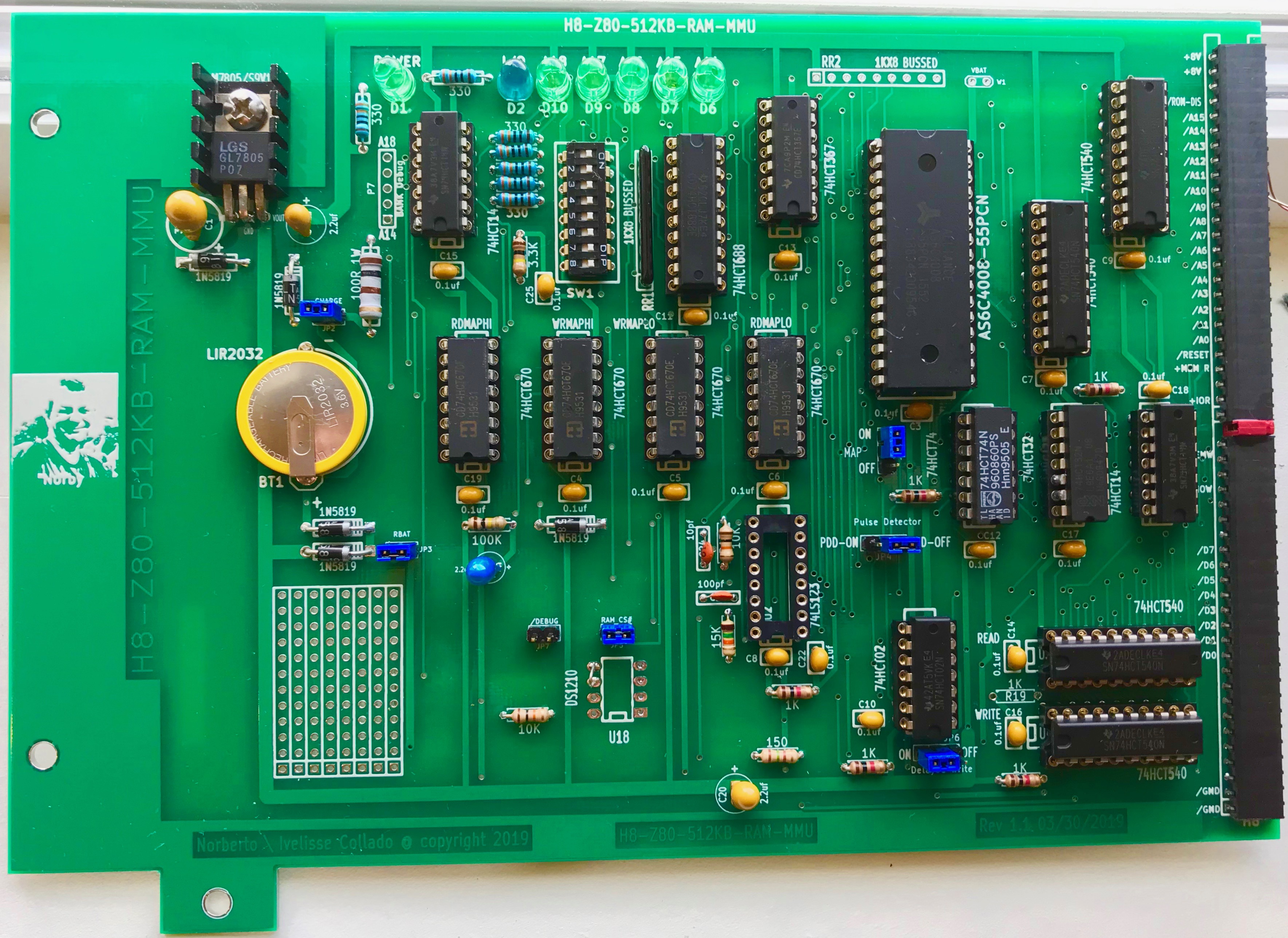
I did receive the 512KB boards this afternoon. That was a very fast delivery. They looked great and will start the assembly of one to check the layout.
See attached picture and will start delivery of them this weekend once verification is completed.
Thanks,
Norby
To view this discussion on the web visit https://groups.google.com/d/msgid/sebhc/B4DC0793-739B-41A9-995F-93C070EB8B44%40koyado.com.
Glenn Roberts
To view this discussion on the web visit https://groups.google.com/d/msgid/sebhc/087D4421-93D5-45A8-8819-677E43040D03%40koyado.com.
<Z80-512K-MMU.jpg>
Norberto Collado
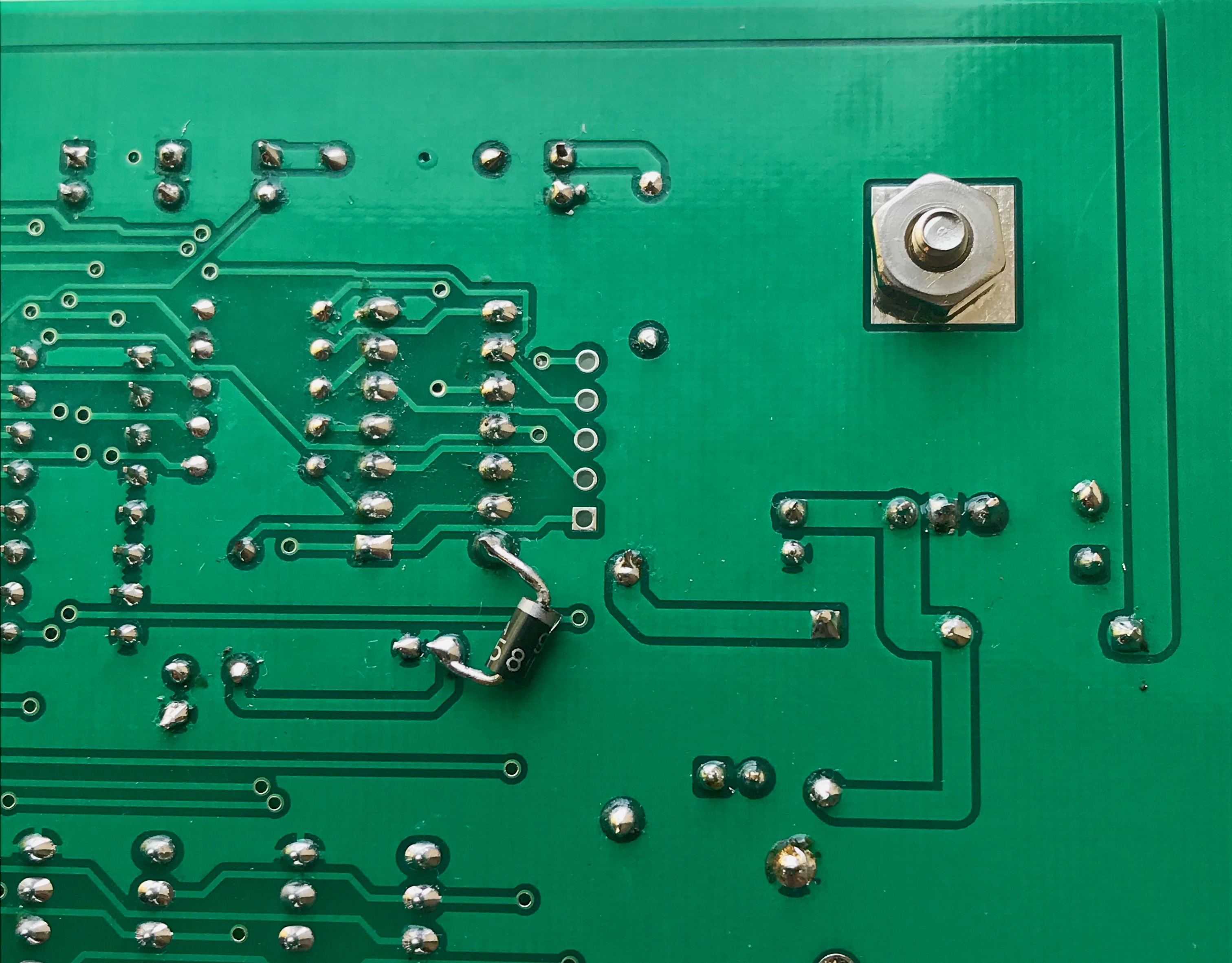
I just finalized the assembly of the H8-512K board and it worked beautifully at 10MHz at position P6. Testing will continue tomorrow and will send out pictures as well.
On my Z80 board setup I removed the on-board RAM (128KB) as it is no longer needed when using the H8-512KB board.
Feedback for the assembly manual.
Z80 On-board RAM (128KB):
Remove On-board RAM from the CPU board.
Circuitry not needed:
Do not install U2 (74LS123), R15 (1K), R16 (15K), C23 (199pf), R17 (10K), C22 (0.1uf), and C24 (10pf). Solder bare wire on JP4 between pins 2 and 3 labeled “PDO-OFF”.
Do not install U18 – DS1210
Do not install “RAM CS#” 2-pin header (JP5)
Install JP7 “/Debug” 2 pin header and add jumper.
Do not install P7 debug 5-pin header
Do not install RR2 – 1K 9-pin Bussed
Heatsink:
Do not install heatsink if placing H8-512K module behind CPU as it will short side 2 of the CPU board. If placing the H8-512KB board at location P6, then you can use the heatsink to keep board secured as long there is not a full size board in front of it as the H8-512KB board is almost half length.
To view this discussion on the web visit https://groups.google.com/d/msgid/sebhc/087D4421-93D5-45A8-8819-677E43040D03%40koyado.com.
Norberto Collado
Attached is a picture of the H8-512KB 100% functional board at 10MHz on slot P6.. As I had to remove the DS1210 because it was acting unstable during power-on, and I had to make other adjustments to the board. CP/M 3 is very stable at 10MHz along with the RAM Drive L:.
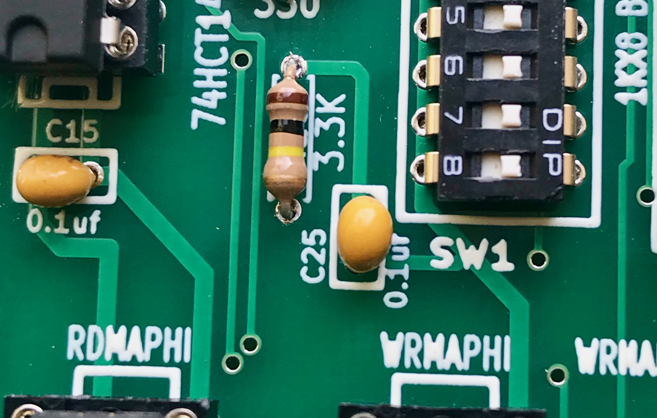
Changes:
Install/solder bare wired between U18 pins 5 and 6.
Replace R18 (3.3K) with a 100K resistor.
Before installing U20 14 pin socket, cut VCC trace to pin 14 (side 1 of the board). Add a diode on side 2 (1N5819) from VCC to pin.
Remove jumper JP7 “/Debug” 2 pin header.
Add jumper JP5 “RAM CS#” for proper operations.
Feedback for the assembly manual.
Z80 On-board RAM (128KB):
Remove On-board RAM from the CPU board.
Circuitry not needed:
Do not install U2 (74LS123), R15 (1K), R16 (15K), C23 (199pf), R17 (10K), C22 (0.1uf), and C24 (10pf). Solder bare wire on JP4 between pins 2 and 3 labeled “PDO-OFF”.
Do not install U18 – DS1210
Do not install P7 debug 5-pin header
Do not install RR2 – 1K 9-pin Bussed
Heatsink:
Do not install heatsink if placing H8-512K module behind CPU as it will short side 2 of the CPU board. If placing the H8-512KB board at location P6, then you can use the heatsink to keep board secured as long there is not a full size board in front of it as the H8-512KB board is almost half length.
Thanks,
Norby.
To view this discussion on the web visit https://groups.google.com/d/msgid/sebhc/247D8293-AA9B-42DA-B8B8-B0ABC3D050DE%40koyado.com.
Norberto Collado
Z80 configured for H8-512KB RAM board (picture attached). Setup is new Z80, H8-512KB, H8-USB, H8-Z37, and H8-Z67. Very reliable setup.
To view this discussion on the web visit https://groups.google.com/d/msgid/sebhc/82C49CCD-E046-4C25-8EB9-6F8B99F953FB%40koyado.com.
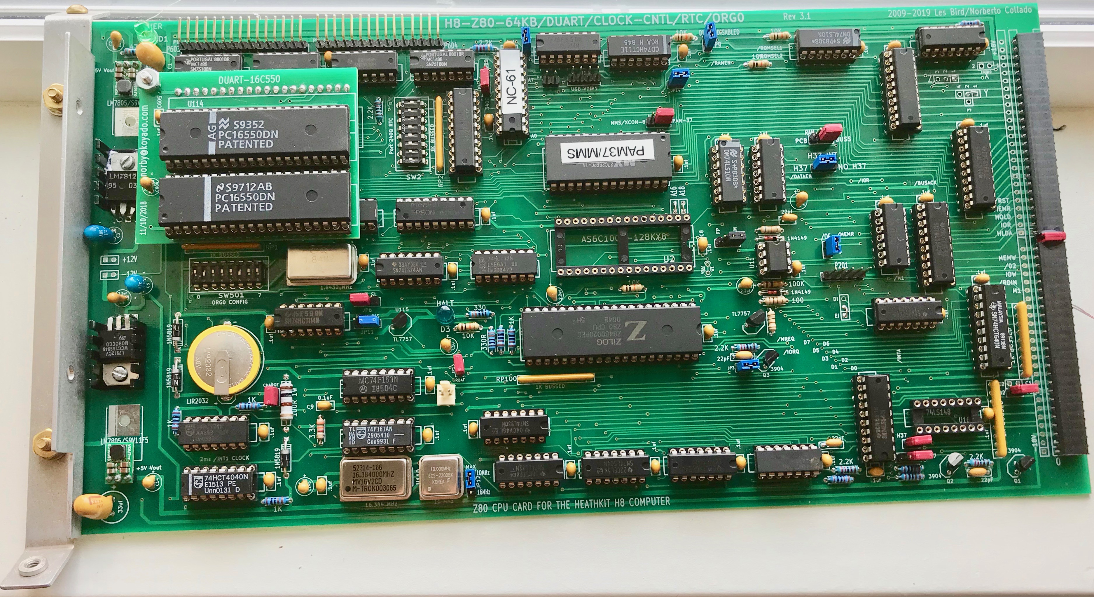
Norberto Collado
Updated H8-512KB board picture as previous one was missing a 1K resistor.
To view this discussion on the web visit https://groups.google.com/d/msgid/sebhc/97C90088-C7DC-48AB-B370-63C4E65B96AD%40koyado.com.
Norberto Collado
Updates:
The H8-512KB ran all night and all day stress tests at 10MHz without any issues. I started today to send out the International Invoices to ship out the remainder Z80, DUART, and the H8-512KB boards.
I have a very robust system with the new Z80 board and the H8-512KB under HDOS, Heath CP/M 2, and MMS CP/M 3.
The remainder board which is the storage board is going to take more time to layout. It is a single board with the H17 controller, H67 Controller, and the H37 controller., using the H89 schematics to cut down on parts. The USB controller will be supported by the Z80/DUART board in the near future.
To view this discussion on the web visit https://groups.google.com/d/msgid/sebhc/3AE92F51-E834-4502-BEB4-56465AA1309B%40koyado.com.
Norberto Collado
To view this discussion on the web visit https://groups.google.com/d/msgid/sebhc/684E3E2F-B7C1-408A-AF5F-CF6450BAA805%40koyado.com.
Glenn Roberts
My 512K board arrived in great shape. Ken and I are working on an Excel BOM sheet… thanks!
- Glenn
To view this discussion on the web visit https://groups.google.com/d/msgid/sebhc/20190329224231.1321cca37f09b4ab87c5049afdc8ceaa.9888ee5bf4.wbe%40email09.godaddy.com.