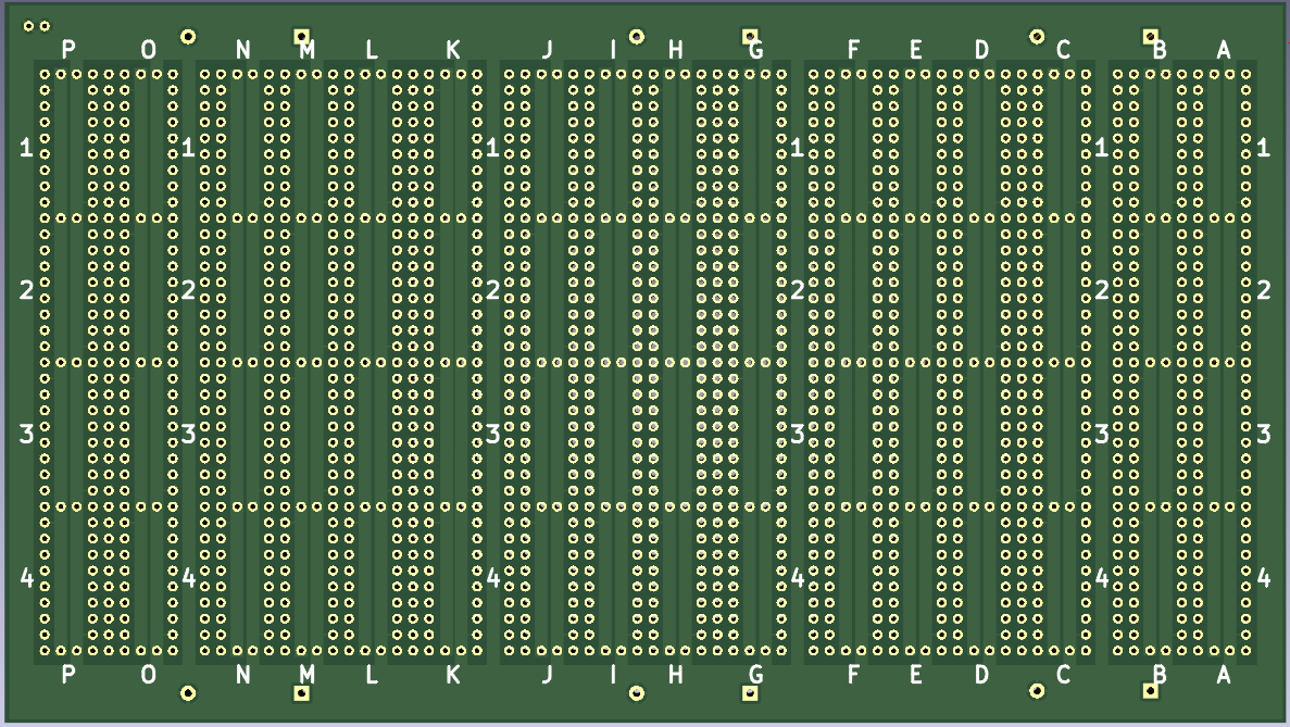
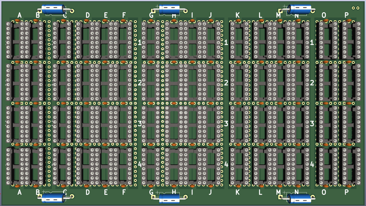
Prototyping PCB patterns

Douglas Miller
prototyping back in the old days at Magnolia Microsystems. Brad Gjerding
had a pattern he used for wire-wrap boards, which he used for his NASA
contracts. He also made some general-purpose PCBs with that pattern that
we used for prototyping. Since I've never seen a pattern quite like it,
and found it very useful, I have created a kicad PCB layout as an
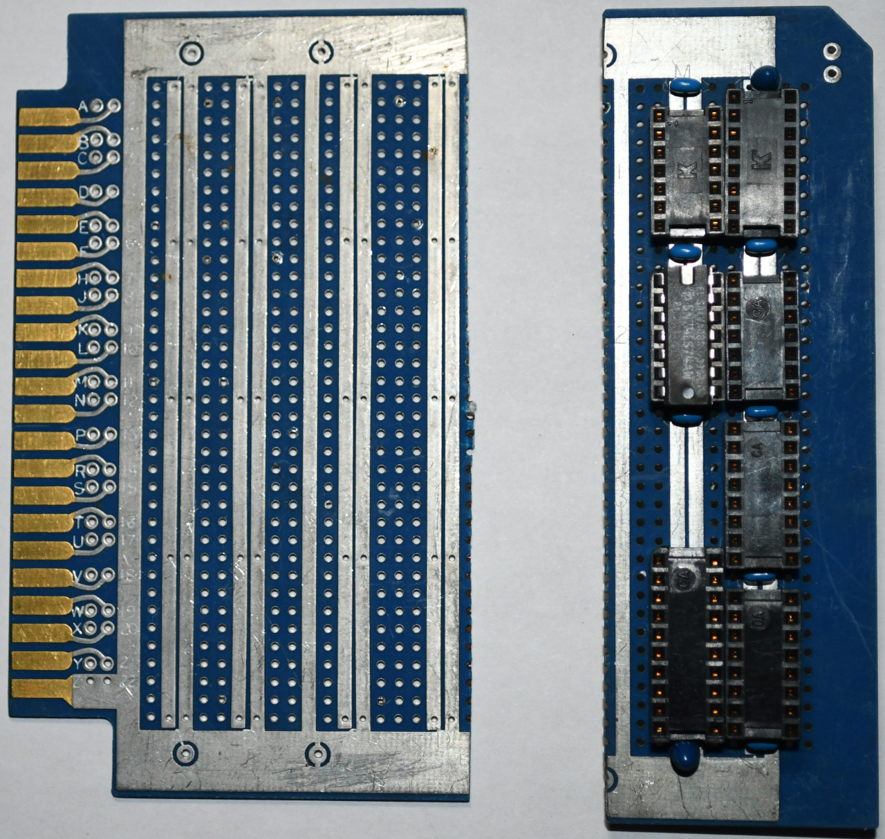
example. Attached are some 3D views plus a photo of some old pieces of
one of those boards.
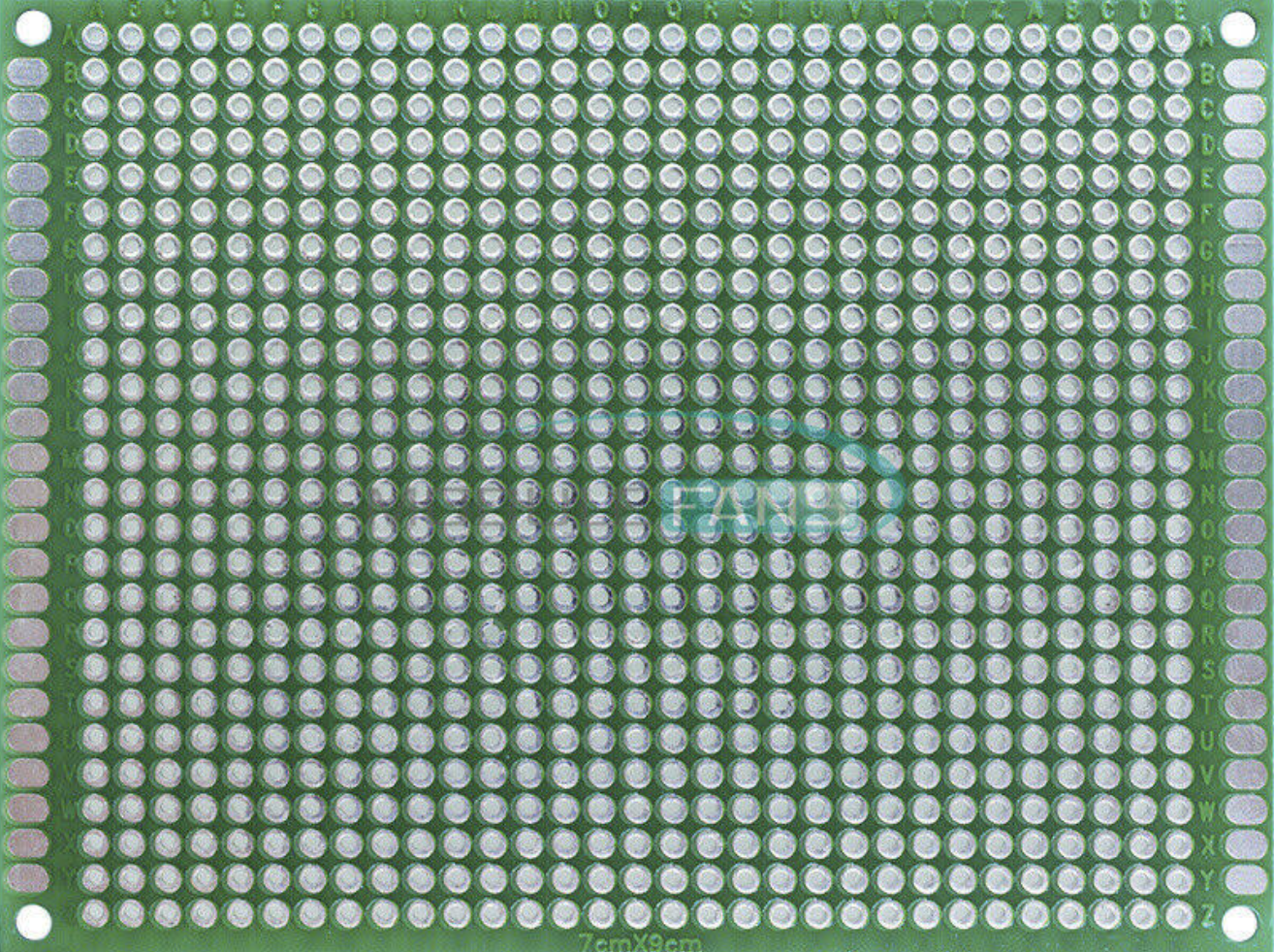
The pattern is intended for wire-wrap, but could probably be modified to
suit other types of prototyping. It can easily accommodate 0.3" and 0.6"
DIP sockets (0.6" only in certain columns) and has a lot of power/ground
foil and is setup for bypass and filter caps. The DIP power/ground
traces default to DIP-16, but those can be easily cut as needed and
power rails are close by for easy connection to any DIP package.
The benefits of the pattern may not be obvious until you've used it, but
I throw it out here as something to think about. I've stored the kicad
project at https://github.com/durgadas311/MmsCpm3/tree/master/pcb/bkg-77000.

Joseph Travis
--
You received this message because you are subscribed to the Google Groups "SEBHC" group.
To unsubscribe from this group and stop receiving emails from it, send an email to sebhc+un...@googlegroups.com.
To view this discussion on the web visit https://groups.google.com/d/msgid/sebhc/2c7edb5a-f900-ade0-5777-31dbf3ea896e%40gmail.com.

glenn.f...@gmail.com
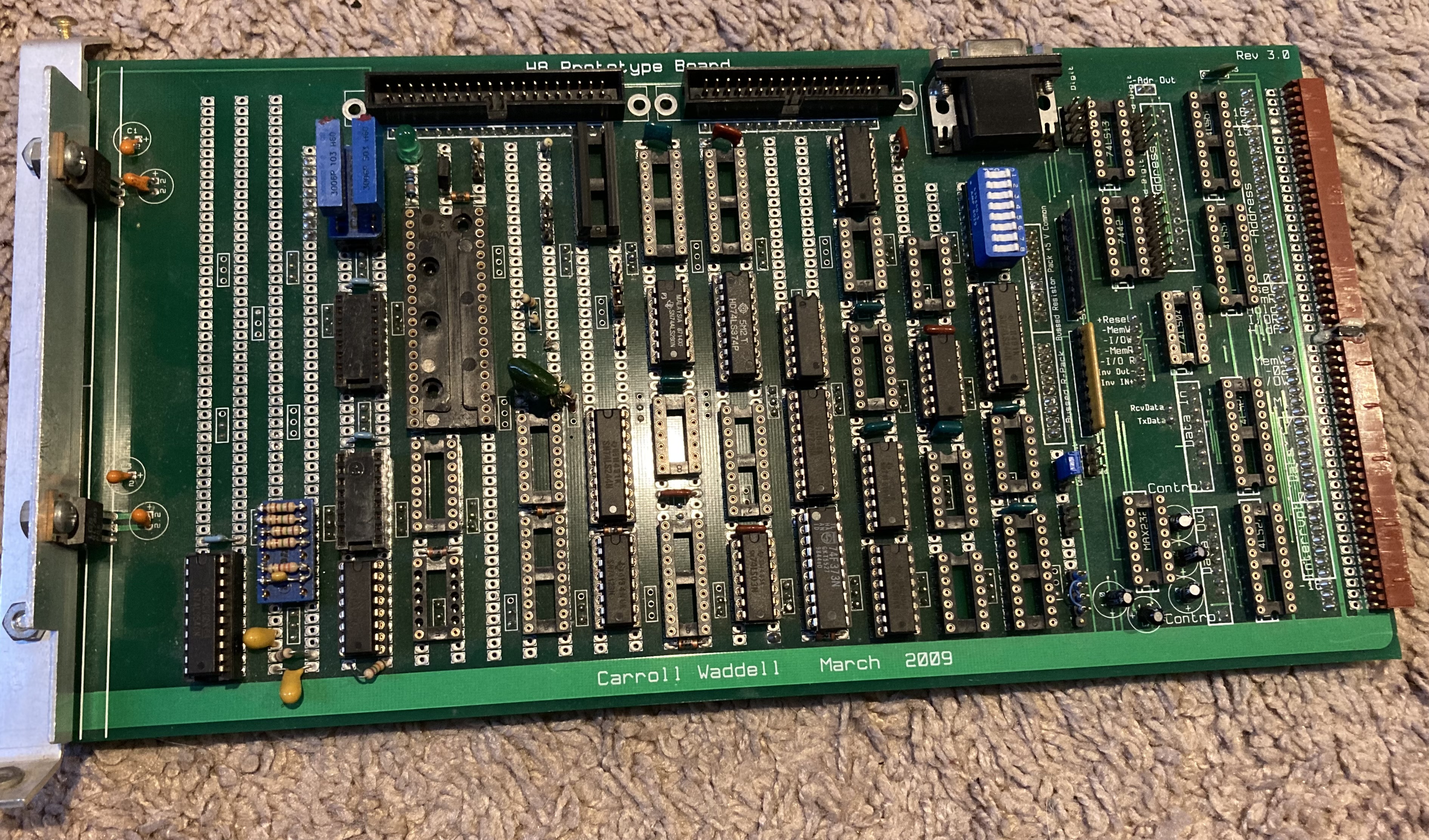
Ed Aumiller, the guy from Virginia from whom I collected some hardware a few years ago, used to use H8-7 prototyping boards as the foundation for mounting protoboards (in his case he used wire wrap boards). He would order the blank H8-7 PCBs from Heath, cut out a rectangular opening and mount the wire wrap board, then use the bus interface logic on the board to interface to the H8. A little crude but effective. He built a number of prototypes this way…
Pix of one of his boards from my rescue:
To view this discussion on the web visit https://groups.google.com/d/msgid/sebhc/CAGQDgBDXCrXZxvrFM4-CPhZRspaLs2iOv5xdRZS6ByvqAzc%2B2g%40mail.gmail.com.
Douglas Miller
I was presenting the pattern as the potential for H8/H89 proto
boards, or for certain boards that have an area set aside for
prototyping (like the WizNet board) or for boards that don't fill
the entire full-sized H8 board. The one board I showed was just
what Brad had created for general experimental use, but the
pattern could be used to fill almost any size board or area. I
first encountered the pattern on full-sized tack-mount boards for
a multi-CPU 6800 system, something like 18"x18".
To view this discussion on the web visit https://groups.google.com/d/msgid/sebhc/003d01d8f9f0%2417a22840%2446e678c0%24%40gmail.com.

norberto.collado koyado.com
Terry S. and I already brainstorm this idea of using a removable proto board on the H8 board as Glenn pictures described. I think this is the way to go to re-use such board as needed. This is in the To-Do-List.
Also, we need to consider that the pattern should support PLCC44 DIP sockets.
Thanks,
Norberto
To view this discussion on the web visit https://groups.google.com/d/msgid/sebhc/13a08438-ebc6-d3b4-73a9-74734e7b661c%40gmail.com.
Douglas Miller
Yes, adding space for a PLCC44 through-hole socket would be good, although then one also wonders about PLCC32 as well, and maybe PLCC68. Perhaps the answer to PLCC packages would be the PLCC-to-DIP adapters, which then would fit into the pattern as-is. Depends on how much PLCC work we think we need.
The PCB I showed was really just a "demo", to visualize the
concept. We can make a PCB of any form-factor using that pattern
(or whatever pattern is needed). Since there are no boards in
existence, we might as well design the board to be what we want.
To view this discussion on the web visit https://groups.google.com/d/msgid/sebhc/SN6PR01MB3855404F816B9CBEF67B8868F7079%40SN6PR01MB3855.prod.exchangelabs.com.
norberto.collado koyado.com
We were considering the attached proto-card to be installed on the H8 wire-wrap board or something similar (picture attached).
I’m more on having the same pattern on the whole board with the +5V and the GND on the outside pattern. Something similar to this:
To view this discussion on the web visit https://groups.google.com/d/msgid/sebhc/30d95f78-4719-52ae-39b0-4f77a76c28f5%40gmail.com.
Douglas Miller
Understood. As I stated earlier, without actually using the pattern I suggested it is difficult to fully appreciate its benefits. I personally prefer a pattern that supplies a strong and stable VCC and GND (which includes easy/clean addition of bypass caps). I'm not sure how much of that is placebo and how much can actually be measured. Part of that depends on whether one is throwing something together "quick and dirty" or whether they actually plan on running it indefinitely. I would argue that if one is building a true prototype - with the intent of transferring to PCB "finished product" - that you don't want to be chasing problems you'd never have on the final PCB. I've been forced to use a lot of "off the shelve" patterns over the years and they always frustrate me. But, I'm not likely to use either design of prototype board, so the decision needs to be left to others. I just present it as a pattern that I prefer over all others that I've seen (so far).
To view this discussion on the web visit https://groups.google.com/d/msgid/sebhc/SN6PR01MB3855841CED565C2C0BC55F3CF7079%40SN6PR01MB3855.prod.exchangelabs.com.

Terry Smedley
norberto.collado koyado.com
The holes pattern described here are for using normal IC sockets for point to point soldering. For Wire-wrapping the holes needs to be bigger.
Here is an example of a wire-wrap IC sockets as holes are bigger. I used this board to develop/test the H37/H67 controllers before production.
To view this discussion on the web visit https://groups.google.com/d/msgid/sebhc/20c1d37d-3ce8-3a6f-5153-9e0d6045d065%40gmail.com.
Douglas Miller
A modular design is interesting, but I worry about the strength of the base board - I imagine, with such a large cut-out, there needs to be some sort of strengthening bars horizontally?
I guess one could design this such that the mounting screws
actually doubled as making the power and ground connections,
thereby providing the best possible conductivity. Possibly,
mounting the "secondary" prototype board might also provide the
mechanical strength needed. Depends on whether the secondary PCB
mounts overlapping the base board, or fits flush inside the
cut-out (harder to do mechanically).
Would there be a set of pads for the H8 bus signals? Or something more formal like a connector (i.e. the base board is sort of like a bus extender)?
What's the cost of a large PCB with a very large cut-out? Seems
like a lot of board material is wasted. I wonder if it is more
cost-effective to just have several layouts available - all with
the same H8-bus-interface circuitry. Sort of "drop-in" patterns
but at the gerber level rather than physical PCBs.
To view this discussion on the web visit https://groups.google.com/d/msgid/sebhc/8a082674-4d0e-4db9-b4bd-08520c6b0246n%40googlegroups.com.
Terry Smedley
Douglas Miller
OK, I was thinking that wire-wrap was still desired, for which
you'd need a cut-out or something. Or else you have to remove the
protoboard from the main board every time you work on it. I guess
the same is true for point-to-point soldering as well, although
one might be expecting to make changes with WW more than soldered
wires.
The only issue I'd see with using a ribbon to connect signals is
just further signal degradation. Even the MMS H89 boards that did
that made me uncomfortable, and I guess Heath did it, too, with
the H37. I guess this ribbon would be ultra-short, but it's also
the connectors themselves that attenuate - perhaps more than the
cable at that length.
To view this discussion on the web visit https://groups.google.com/d/msgid/sebhc/768c1a57-71c5-44cf-9712-c9d188a8b9c7n%40googlegroups.com.