SC126 assembly and fault finding
237 views
Skip to first unread message

Derry UK
Nov 28, 2021, 6:23:04 AM11/28/21
to retro-comp
Just looking for guidance with assembly of this PCB.
I have inserted the resistors, IC sockets and clock crystal and at a test point and the build instructions say "
Connect the meter probes to each terminal of one of the capacitors, such as C1. This should be an open circuit, not a short."
Mine isn't open circuit but nominally 10K, it varies slightly depending on where I test on the PCB.
I realise 10K insn't a short but is 10K OK or do I have an issue?
Thanks,
Derry.
Derry UK
Nov 28, 2021, 11:23:19 AM11/28/21
to retro-comp
Problem solved.
My first thought was if I was going to start fault finding it would be nice to start with a clean PCB ie no flux residue. So I put the PCB in the dishwasher and selected "Quick and clean 60 deg C".
Result now when I check C1 is 33M ohm. We live and learn.
Derry.

Richard Deane
Nov 29, 2021, 3:35:23 AM11/29/21
to Derry UK, retro-comp
Was that in dishwasher with plain water or did you use detergent?
--
You received this message because you are subscribed to the Google Groups "retro-comp" group.
To unsubscribe from this group and stop receiving emails from it, send an email to retro-comp+...@googlegroups.com.
To view this discussion on the web visit https://groups.google.com/d/msgid/retro-comp/e02af76c-87ba-42bb-8782-e3fab6184ccan%40googlegroups.com.
Derry UK
Nov 29, 2021, 4:48:40 AM11/29/21
to retro-comp
With detergent.
It seems to me that if you don't use detergent you might as well hold the PCB under a running tap.

Kevin Price
Nov 29, 2021, 4:57:06 PM11/29/21
to retro-comp
I've noticed the SC boards are very fragile like that. I try to keep those boards in packaging/an enclosure because it does not take very much at all to expose the copper.
My original PIO board I destroyed the ground trace when the soldering iron scraped it. He does sell bare boards though. The official boards, and Kamprath' Hacks versions of JB langston designs seem to have some kind of conformal coating.

Steve Cousins
Nov 29, 2021, 6:46:03 PM11/29/21
to retro-comp
Interesting. My boards are manufactured by JLCPCB and as far as I'm aware they are considered good robust boards.
I deliberately use relatively wide tracks to help make them robust and resistant to accidental damage. I try to avoid the very narrow tracks that look very fragile to me. My more recent designs also try to avoid running tracks between pins on the solder side to help reduce the chance of damage during soldering. I also generally add teardrops where the tracks meet the pads, which is a weak spot, especially with narrow tracks.
These precautions are just my desire to make my kits suitable for those with little soldering experience, it is not because I've experienced problems myself or had reports of problems. My goal is to produce kits that are reliable projects even for those with little experience.
As best I remember the only issues I've had reported are the difficulty in soldering ground pins when there is a large ground plane around them. Since hearing this I use much thinner 'spokes' which should help.
As for the solder resist layer, I'm not aware of any issues relating to it.
I would be interested to hear any opinions anyone has about the issues mentioned.
Steve

Jeff Greer
Nov 29, 2021, 7:17:00 PM11/29/21
to Steve Cousins, retro-comp
I have built several SC kits. The boards are high quality and assemble as expected according to the assembly instructions. I have had a SC126 and several expansion boards for 2+ years. The SC126 is the main RC2014 type computer that I use. I use it several times per week with no issues.
It is not a beginner kit but careful assembly with a quality soldering iron.
Jeff
To view this discussion on the web visit https://groups.google.com/d/msgid/retro-comp/1704c00e-b1a6-4743-8b44-3d848735cde2n%40googlegroups.com.

Dylan Hall
Nov 29, 2021, 8:30:43 PM11/29/21
to retro-comp, Steve Cousins
I've been really impressed with the SC kits. I'm a little biased as I consider the quality of the documentation second to none so I may be looking more favourably on the PCB's as a result :)
I did hit an issue with a non-SC kitset where I wanted to replace a resistor because the power LED was way too bright. I ended up damaging the board trying to remove the solder from the hole after I had extracted the resistor legs. I think the modern PCB's with through-hole-plating (is that the right name for it?) make removing things much harder.
Dylan
To view this discussion on the web visit https://groups.google.com/d/msgid/retro-comp/CALnunYJP%3DuMOXX%2B3OxRC1FGc48PemgPJs_0XbmbiuPLmq6oCRQ%40mail.gmail.com.
Dylan Hall
Nov 29, 2021, 8:35:02 PM11/29/21
to retro-comp, Steve Cousins
I'd like to add another thought, a big thanks to Steve for having his PCB designs publicly available on EasyEDA. As someone new to making PCB's I've found using them as a reference hugely useful (what is a sensible track width, how close is it ok to place parts, etc). I've also borrowed many of the parts from your library :)
Dylan
Kevin Price
Nov 29, 2021, 8:40:19 PM11/29/21
to retro-comp
I'm attaching a picture of the shows the kind of damage that I've caused. Emphasis is on me causing the damage, not that the boards are poorly designed or manufactured.
The issue isn't with the boards themselves - it's that *I've* needed to be careful in a way that I've never needed to worry about. It was surprising as I've done a lot of soldering of microcontroller kits and breakout boards - most of the boards from adafruit/sparkfun/etc seem to have a coating on them or use a different manufacturing process. I've never exposed copper or blown a trace before.
I absolutely love your kits and I've likely spent over $200 in your store since July.
Kevin Price
Nov 29, 2021, 9:14:40 PM11/29/21
to retro-comp
To clarify the reason they seemed fragile to me - I'm used to working with boards that are coated with something so you can accidentally stab them with a screwdriver during assembly. I think your boards are of the same type that I've seen in pre-assembled hobbyist stuff I've bought like a a GB8K upscaler, and a replacement CRT RGB input driver for a tube television.
Steve Cousins
Nov 30, 2021, 5:14:33 AM11/30/21
to retro-comp
Thanks everyone for the comments.
It can be very helpful looking at PCBs designed by other people. I would recommend taking a look at designs by J.B. Langston, Phillip Stevens, Bill Shen, and any others you can find. These 3 have very different looking results and their designs are very impressive. There is always something to learn.
Anyone looking at my boards should note the comments I made earlier about my use of "unnecessarily" wide tracks. I also generally keep component and track spacing above the minimum supported by the PCB manufacturer.
Another thing I usually do is increase the size of via holes above the default in EasyEDA (and above the minimum supported by JLCPCB). I increase the hole size and the pad size. This does limit the density of tracks you can run but most of my designs are not very densely packed so it is not usually a problem. Some designers try hard to reduce the number of via holes down to none (in some cases). I don't make this a priority as it often involves running more tracks between pins. I consider doing that on the solder side to add more risk than additional via holes.
Most of my recent designs have these minimums set as design rules:
Track width 12 MIL
Clearance 12 MIL
Via pad diameter 32 MIL
Via drill diameter 16 MIL
Keeping well above the PCB manufacturer's minimum should avoid manufacturing tolerance issues resulting in fragile and unreliable PCBs. As a kit supplier, I really don't want my designs to carry those risks.
Because I design kits to be assembled and understood by people with a wide range of skill levels I have different priorities to many others here. I generally avoid changing 'obvious' pin associations to simplify the layout, such as maintaining the relationship of address and data lines to RAM chip pin names. I try to keep all the ICs facing the same way to reduce the possibility of confusion. I put a lot of effort into useful labels and information on the silkscreen. I want the components well spread out, where possible, to make assembly easier.
I was very pleased with SC114 as all 5 chips have a different number of pins so you can't put the chips in the wrong place by mistake. A little thing but it removes one more small risk. I'm tempted to redesign the PCB though to bring it up to my latest thinking.
Another thing I like is to completely fill the unused areas with a copper fill (or ground plane). If you do a good job on the power supply routing the ground plane is not generally required for these types of circuits but I like the look of them. A lot of copper also gives them a slightly heavier and more robust feel.
Another thing I avoid is sharp 'concave' angles both on track routes and where they join pads. Many years ago (around 1982 I think) I was involved in PCB manufacturing equipment. A few things that concerned the production guys, such as acid traps, influence my current designs. I assume production equipment and techniques have improved but the same issues may still exist to some extent. Acid traps are where acid from the etching process gets trapped in tight spaces and continues to etch away the copper for longer than it should. Narrow tracks are particularly vulnerable to damage here.
One of the reasons I increase the via hole size is from that long-ago experience. The thought of trying to plate those tiny holes fills me with the suspicion that the plating will be very thin and thus a weak point. I try to avoid via holes in tracks carrying any significant current, such as power lines, but when I do need them I usually use several via holes to increase the copper area. Back in the day the quality control guys took daily PCB samples and measured the force required to rip the plating out of a via hole. I wonder if they still do that.
I while back I wrote a sort of beginner's guide to designing using EasyEDA. It might be a bit dated now as EasyEDA is continually evolving but some may find it useful.
If you have any interest in designing PCBs I highly recommend giving it a try. It can be very satisfying, especially when you get your brand new masterpiece turn up in the post from the PCB manufacturer. Just watch out for PCB design addiction - it is a thing!
I didn't rediscover retrocomputing with the aim of selling kits. I just sort of drifted into it. Now it uses up most of my playtime. My original goals seem to have been put on hold :(
Steve

Tom Szolyga
Nov 30, 2021, 2:09:00 PM11/30/21
to retro-comp
A board is "Fragile" if it does not survive stabbing with a screwdriver? Really? Here is a thought: stab you car with a screwdriver. If the car is damaged, your car is "fragile".
I have used Steve's boards from the very beginning. None, not one, has ever failed. In fact I purchase on eBay a bad 40 pin dip chip. I unsoldered it from a board and soldered on a new one. All pads and traces survived and the board worked fine. I suggest removing the cylinder heads from your car's engine, replace them it with new ones, accidentally stab a rocker arm with a screwdriver and test starting the car. If it does not run, your car is "fragile".
Bottom line: If you want to "stab" your PCB's, dip them in epoxy.
Kevin Price
Nov 30, 2021, 8:13:44 PM11/30/21
to retro-comp
Actually Tom, epoxy is commonly used as a conformal coating to protect against abrasive damage. I have not stabbed a board from SC with a screwdriver. The only board I have stabbed with a screwdriver has been my PC main board, without any damage.
I recorded a demonstration of taking lineman's scissors to an epoxy coating: Example of epoxy.
I recorded a demonstration of taking lineman's scissors to an epoxy coating: Example of epoxy.
Even comparing different rc2014 cards the coating on my (still very excellent) SC cards is thinner and does not even up the depth between the traces.
Coming from the rc2014 classic ][ (which I did not put in a case for the first month) and the above, SCs boards are more susceptible to the kind of damage (exposed copper on the traces) that I posted a picture of. This is due to different coatings, and it may well be that the boards I experienced this with had their coatings innapropriately applied or set - covid has changed a lot about quality control.
I do not have a mechanism to precisely apply force, but a light swipe with those same lineman's scissors in a cutting motion goes into the cladding on my SC115, but leaves a light white mark on teh 32k ram board from my classic ][ - which is going to come down to a difference in coating.
Relative to other boards I have assembled and used, Steve's boards aren't as tolerant to abuse. So be careful, store them carefully, and keep them in an enclosure/prevent the pcb surface from coming in contact with anything. I definitely would not advise running them through the dishwasher (detergent or no) if there was a chance the surfaces of the board could experience vibration or friction against any surface in the dishwasher. In retrospect I realized that many people here would not consider them fragile at all, whereas most of the people at my hackerspace would and I've tried to clarify that.
Kevin Price
Nov 30, 2021, 8:26:41 PM11/30/21
to retro-comp
Also, If it hasn't come across clearly - I'm a giant fan of Steve's Kits and would tell anyone to buy one, but make sure they have an enclosure ready to go and select a soldering tip that's unlikely to leave a scratch.
In the last four months I've bought and assembled an sc130, sc126, sc104, sc108,sc112, sc104, sc113, and a sc118. I would not have done that if these kits weren't superb.
In the last four months I've bought and assembled an sc130, sc126, sc104, sc108,sc112, sc104, sc113, and a sc118. I would not have done that if these kits weren't superb.

Tadeusz Pycio
Dec 1, 2021, 2:18:25 AM12/1/21
to retro-comp
Coming from the rc2014 classic ][ (which I did not put in a case for the first month) and the above, SCs boards are more susceptible to the kind of damage (exposed copper on the traces) that I posted a picture of. This is due to different coatings, and it may well be that the boards I experienced this with had their coatings innapropriately applied or set - covid has changed a lot about quality control.
Interestingly, I have some PCBs from Steve and each one looks like new, with no defects or scratches. If I remember correctly, these projects are available, so there is nothing to prevent them from being made in a factory that meets the required expectations.
Kevin Price
Dec 1, 2021, 5:56:06 PM12/1/21
to retro-comp
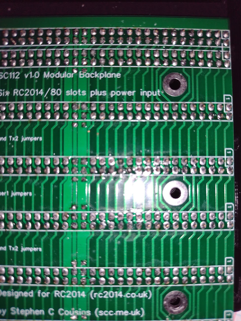
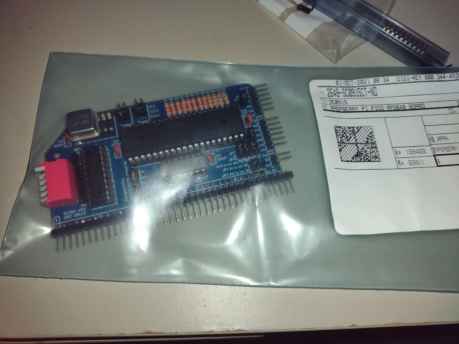
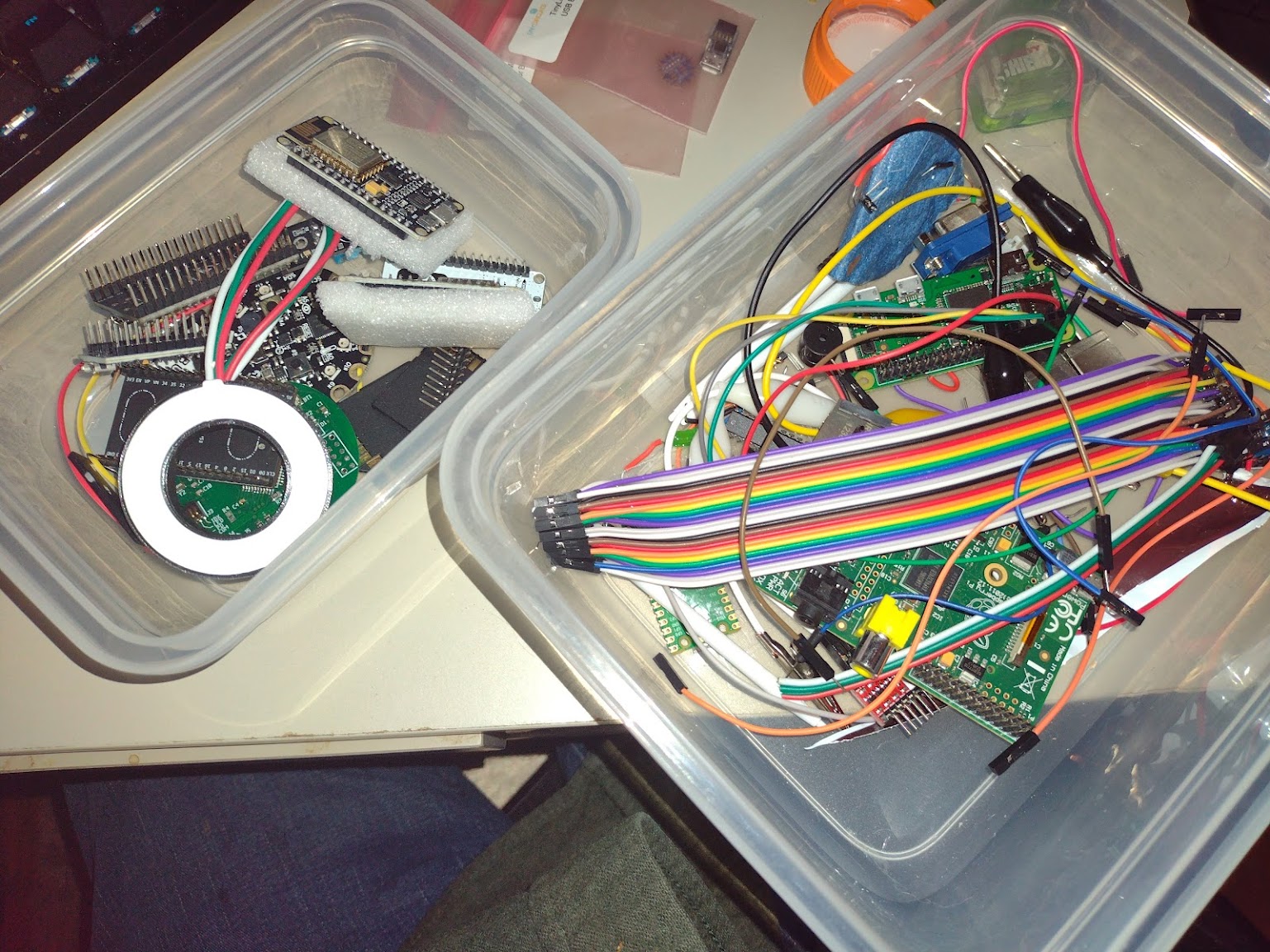
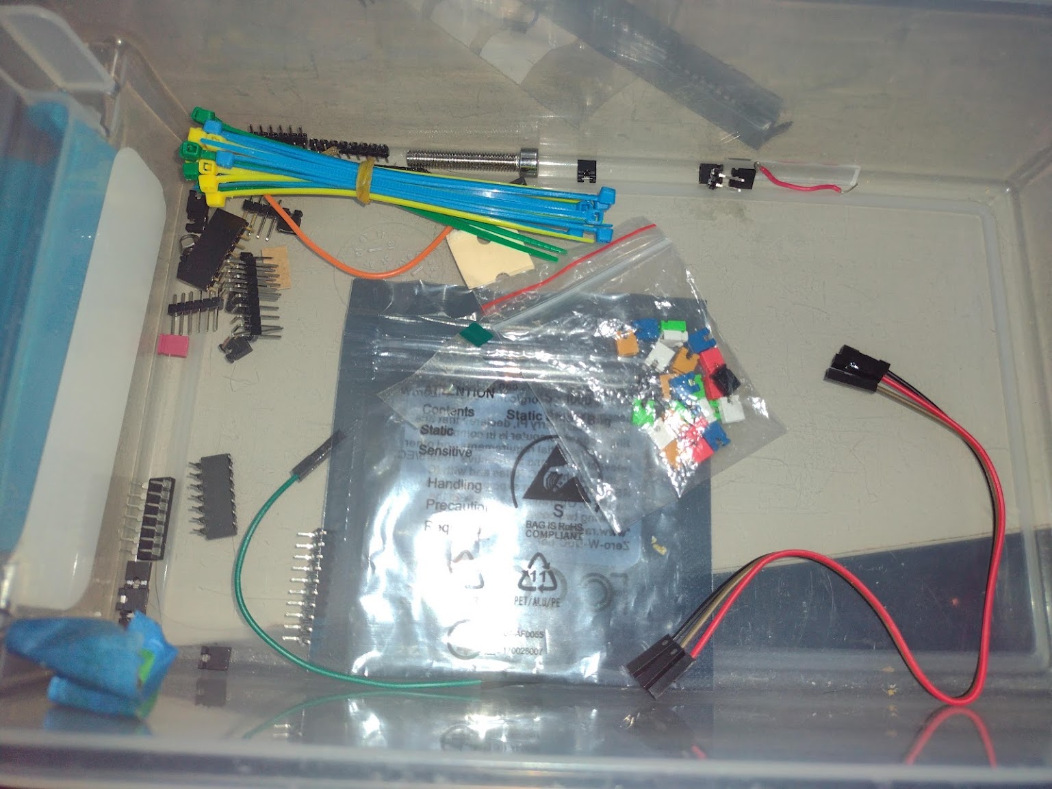
I'm going to reply one last time because I *know* besmirched Steve with a poor choice of words in my initial comment. As someone who came to this side of hobbyist electronics from 3d printing and general making, I was not accustomed to the care needed. The picture with two boxes is how I am accustomed to storing soldered together boards and components. The picture of the box with the odds and ends is the box both the rc2014 classic ][ and the sc112 were in when I noticed the copper had become exposed. The final picture is how I store Steve's kits now - because they are awesome and I value them.
To people coming from a class of product you can carry in your pocket for a week (try it with a pi zero, just brush the lint off first), or will survive the conditions in a wood or metal shop - it was surprising. Relative to the above arduino, or a DIY mach3 stepper board they seemed fragile. I know a lot of people under 30 who would be equally suprised.
In the same way, I realize static is a major risk with many of these chips - that's not something I've had to take into consideration. At one point after someone made a miniature van-degraff generator we had a competition to see if anyone could kill a development board by touching it. It escalated to trying to kill PC components and that was unsuccessful too.
I've attatched a simple remix of Jim Mcinnis' sc113 sled so the sc112 fits.
Reply all
Reply to author
Forward
0 new messages