HV5530 problems
494 views
Skip to first unread message

gregebert
Oct 5, 2018, 3:48:33 PM10/5/18
to neonixie-l
I'm starting a separate thread on this topic that was posted from the introduction discussion
As with any serial shift-register, the biggest source of trouble is timing-related, such as not accounting for setup and hold-time requirements.
First question: Are you able to get reliable and predictable data into the first HV5530 that is connected to your controller ? If not, then the entire shift chain will be broken, aka "garbage-in, garbage out".
This needs to be solved first. I took a quick look at the code that was posted and did not see any obvious issues, so I think your setup/hold timing getting into the first HV5530 is correct.
Do you have level-shifters between your controller and the HV5530 ? The logic portion of the HV5530 is intended to operate at 12V, whereas most controller devices have 3.3V logic levels.
If you dont have a level-shifter, then you are operating outside the device spec and you venturing into a jungle of unpredicatbles and uncontrollables.
I know some neonixie members have posted about their good results with HVxxxx devices operated outside of spec, so if you are adventurous then go for it.
All I can say, based on my own experience, is that when you are not datasheet compliant, expect trouble. I had 3 completely unrelated problems with a 16-channel A/D converter on my current project, and all of them turned out to be either my misinterpretation of the datasheet, or my failure to pay attention to a detail in the datasheet. Once I got those corrected, it's been fine ever since.
Second question: If the first HV5530 is operating as expected, what about the next one in the chain ?

Kevin A.
Oct 7, 2018, 6:13:07 PM10/7/18
to neonixie-l
Yes, I am able to produce reliable results between all of my shift registers. A very basic code I got to works was to simply turn off all the latches and then turn them on one by one again. By referring to the truth table for the HV5530 on page 10 of the manual: http://ww1.microchip.com/downloads/en/DeviceDoc/20005851A.pdf, I've been able to achieve the following:
You can see in this code, which HV chip controls which display device on my board. I've done by best to annotate this code in a sensible way, especially the part where I explain each connection to the HV outputs on the 5530's.
First, when my device is powered on, I blank all the outputs by calling the BlankDisplay() function. Then, I turn all of the latches on one-by-one using the transparent latch mode at the bottom of the truth table, which turns each high voltage output on sequentially, while the previous iteration remains in the last state (if turning on, then previous outputs remain on). Here is the code for what I just described:
#define LATCH 10#define CLOCK 13#define DATA 11#define PWM 9
void setup(){ pinMode(LATCH, OUTPUT); // Latch is pin 10, FALLING edge copies shift register to latches pinMode(CLOCK, OUTPUT); // Clock is pin 13, FALLING edge clocks in a bit from DATA pinMode(DATA, OUTPUT); // Data is pin 11 pinMode(PWM, OUTPUT); // PWM (Blank) is pin 9
digitalWrite(LATCH, HIGH); digitalWrite(CLOCK, HIGH); digitalWrite(DATA, HIGH); digitalWrite(PWM, HIGH);
delay(10); BlankDisplay(); LightDisplay();}
void BlankDisplay(){ // Disconnect shift register from data latches: digitalWrite(LATCH, LOW);
// Set the data to LOW digitalWrite (DATA, LOW); // Clock in the LOW 128 times for (uint8_t i = 0; i < 128; i++) { digitalWrite(CLOCK, LOW); // Clock in one data bit digitalWrite(CLOCK, HIGH); digitalWrite(LATCH, HIGH); // Bring the latch high to copy the shift registers to output latches
}}
void LightDisplay(){ // Disconnect shift register from data latches: digitalWrite(LATCH, LOW);
// Set the data to LOW digitalWrite (DATA, HIGH); // Clock in the LOW 128 times for (uint8_t i = 0; i < 128; i++) { digitalWrite(CLOCK, LOW); // Clock in one data bit digitalWrite(CLOCK, HIGH); digitalWrite(LATCH, HIGH); // Bring the latch high to copy the shift registers to output latches
delay(20); // Slow this step down by 20ms so we can see each output turning on
}}
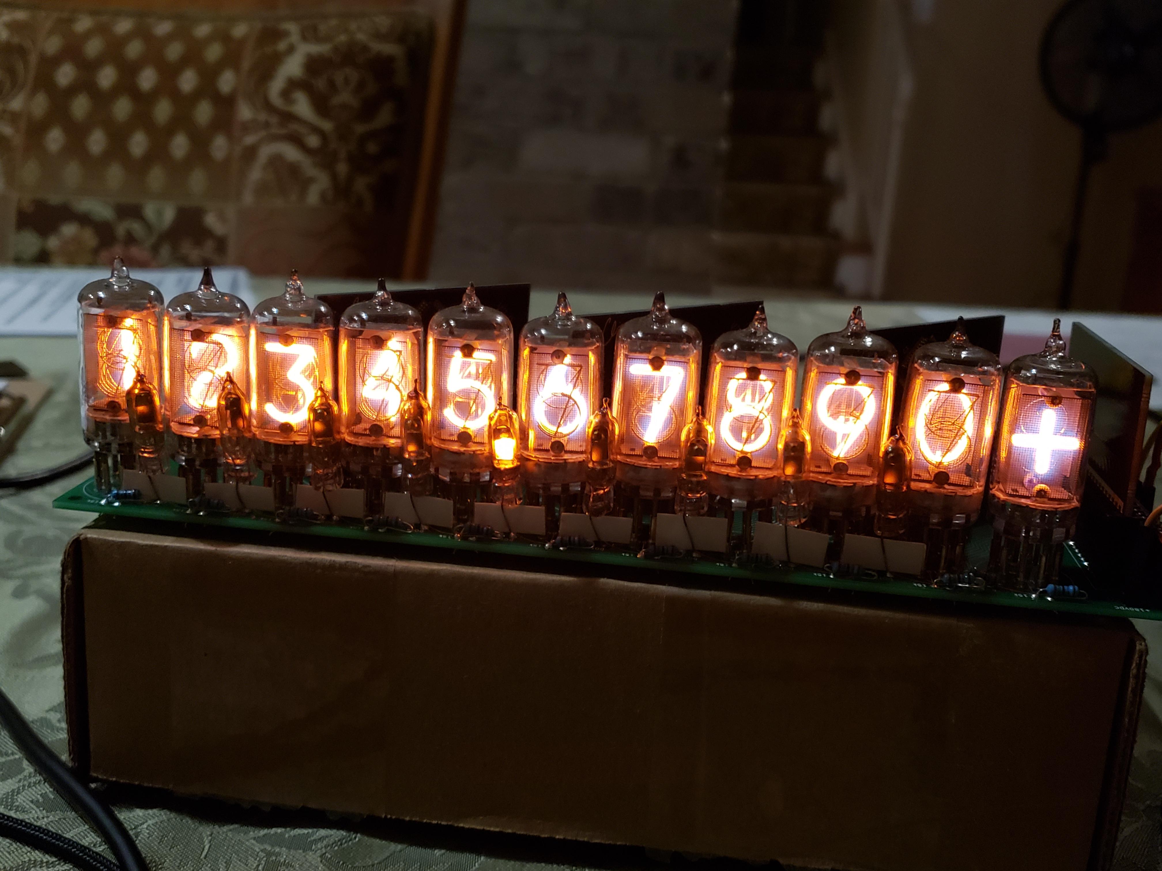
void loop() {//nothing}Here is a quick video to demonstrate the above code running:
I do have a logic level shifter to convert the 12 volt logic from the HV5530 chip to 3.3v logic for the arduino. I have incorporated a Sparkfun sparkfun bob-12009 logic level shifter on my pcb, which can be see here (the logic level shifter is in the upper left hand corner):
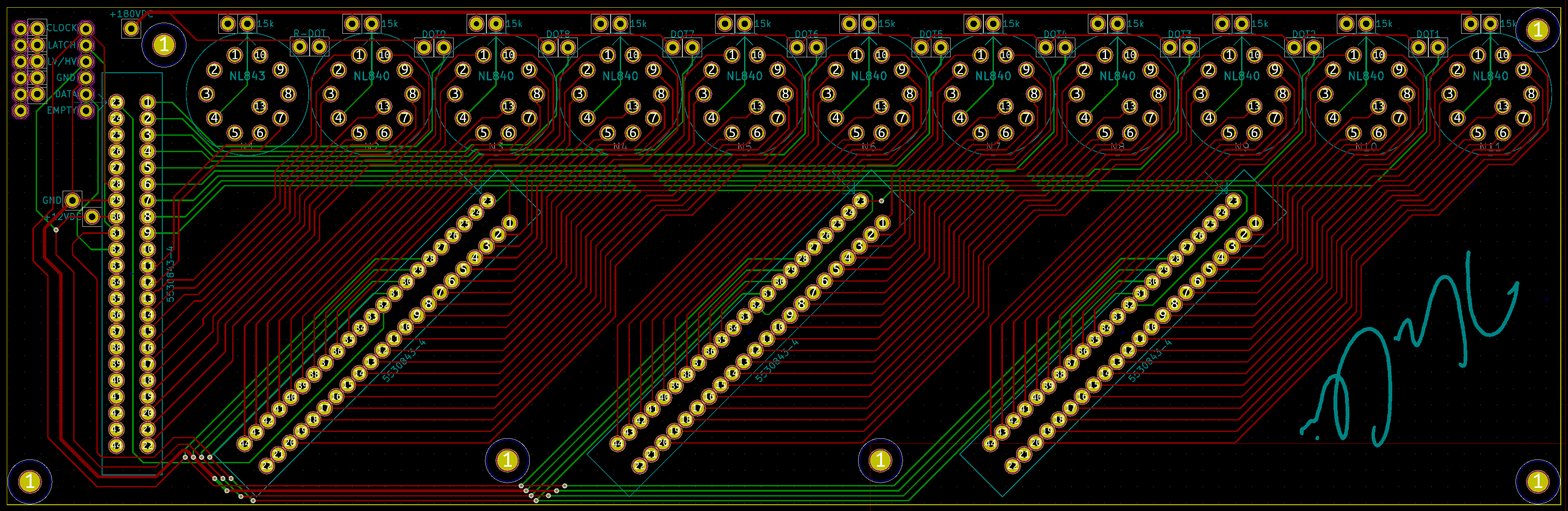
My power supply is an APD (American power design) S10-180, which takes 12 volts DC in and kicks out 180 volts. I have 12 volts from by wall-adapter going to the PSU and directly to the HV logic chips.
I believe my setup is fine electrically, so my problem lies in writing software to make this work.
The most promising code I've found so far was for nixie clock project, which can be found here: http://makerangst.com/nixie-clock-3
This gentleman's code drives the HV5530 chips by tabulating the outputs for each of his tubes in an array, each digit corresponding to an output on the HV chip as defined by the physical connections between the tubes and the drivers. I have tried to adapt his code by writing the following:
#define PIN_LE    10 //Shift Register Latch Enable#define PIN_CLK   13  //Shift Register Clock#define PIN_DATA  11  //Shift Register Data#define PIN_BL    9  //Shift Register Blank (0=display off     1=display on)

// lookup tables for the high and low value of mins/sec to determine// which number needs to be displayed on each of the minutes and seconds tubes// e.g. if the clock is to diplay 26 minutes then it // will look up the values at the 26th position and display a 2 on the high mins tube and a 6 on the low mins tubeconst byte minsec_high[]= {0,0,0,0,0,0,0,0,0,0,1,1,1,1,1,1,1,1,1,1,2,2,2,2,2,2,2,2,2,2,3,3,3,3,3,3,3,3,3,3,4,4,4,4,4,4,4,4,4,4,5,5,5,5,5,5,5,5,5,5,11};const byte minsec_low[] = {0,1,2,3,4,5,6,7,8,9,0,1,2,3,4,5,6,7,8,9,0,1,2,3,4,5,6,7,8,9,0,1,2,3,4,5,6,7,8,9,0,1,2,3,4,5,6,7,8,9,0,1,2,3,4,5,6,7,8,9,11};
// shift register positions// --------------------------HV5530 #1--------------------------// Controls 9 Dots (One cathode each), Plus/Minus tube (2 cathodes), One 10 digit tube (10 cathodes)
// Dots are first//      Dot   1  2  3  4  5  6  7  8  9int dots[] = {1, 2, 3, 4, 5, 6, 7, 8, 9};
//HV5530 #1 Pin 10 (HVOUT20) is not used
// Plus/minus tube  +   -int plusminus[] = {11, 12};
// Rightmost numeric tube (Tube 1)//        Digit  0   1   2   3   4   5   6   7   8   9//  NL840 Pin #  13  5   7   10  6   2   8   1   3   9 int tube1[] =  {16, 17, 19, 22, 18, 14, 20, 13, 15, 21};              //Pins 35-44 (HVOUT1 - HVOUT10) are not used
// --------------------------HV5530 #2,3,4--------------------------//HV5530#2,3,4 each control three (3) numeric tubes each (10 cathodes each, 30 cathodes total)//Connections are similarly numbered between each set of tubes and HV chip for chips 2,3,4//Pins 21 and 22 (HVOUT31 and HVOUT32) are not used
// Next 3 tubes from right to left (Tubes 2,3,4)//       Digit  0   1   2   3   4   5   6   7   8   9// NL840 Pin #  13  5   7   10  6   2   8   1   3   9 int tube2[] =  {16, 17, 19, 22, 18, 14, 20, 13, 15, 21}; int tube3[] =  {4, 5, 7, 10, 6, 2, 8, 1, 3, 9}; int tube4[] =  {41, 40, 38, 35, 39, 43, 37, 44, 42, 36};
//       Digit  0   1   2   3   4   5   6   7   8   9// NL840 Pin #  13  5   7   10  6   2   8   1   3   9 int tube5[] =  {16, 17, 19, 22, 18, 14, 20, 13, 15, 21}; int tube6[] =  {4, 5, 7, 10, 6, 2, 8, 1, 3, 9}; int tube7[] =  {41, 40, 38, 35, 39, 43, 37, 44, 42, 36};
//       Digit  0   1   2   3   4   5   6   7   8   9// NL840 Pin #  13  5   7   10  6   2   8   1   3   9 int tube8[] =  {16, 17, 19, 22, 18, 14, 20, 13, 15, 21}; int tube9[] =  {4, 5, 7, 10, 6, 2, 8, 1, 3, 9}; int tube10[] =  {41, 40, 38, 35, 39, 43, 37, 44, 42, 36};


void setup() {
  pinMode(PIN_LE,  OUTPUT);  pinMode(PIN_BL,  OUTPUT);  pinMode(PIN_DATA,OUTPUT);  pinMode(PIN_CLK, OUTPUT);
  digitalWrite(PIN_BL, LOW);
  Serial.begin(115200);
}

unsigned long previousSRMillis = 0;    // keeping track last time shift register values were clocked in
void loop() {
delay(100);digitalWrite(PIN_BL, HIGH);
  unsigned long currentMillis = millis();    if (currentMillis - previousSRMillis >= 1000) {  // clocking in 1 times a second        previousSRMillis = currentMillis;
    boolean srBuffer[128] = {0};
//    time_t now;//    struct tm * timeinfo;//    time(&now);//    timeinfo = localtime(&now);
        int seconds1 = 1;    int seconds2 = 2;    int seconds3 = 3;    int seconds4 = 4;    int seconds5 = 5;    int seconds6 = 6;    int seconds7 = 7;    int seconds8 = 8;    int seconds9 = 9;    int seconds10 = 10;
    // doing the lookups for what number to display then    // looking up which shift register position    // for each tube    // "10" from the lookup table indicates to blank the tube since it is out of range.        srBuffer[dots[minsec_low[1]] - 1] = 1;    srBuffer[plusminus[minsec_low[1]] - 1] = 1;    srBuffer[tube1[minsec_low[seconds1]] - 1] = 1;    srBuffer[tube2[minsec_low[seconds2]] - 1] = 1;    srBuffer[tube3[minsec_low[seconds3]] - 1] = 1;    srBuffer[tube4[minsec_low[seconds4]] - 1] = 1;    srBuffer[tube5[minsec_low[seconds5]] - 1] = 1;    srBuffer[tube6[minsec_low[seconds6]] - 1] = 1;    srBuffer[tube7[minsec_low[seconds7]] - 1] = 1;    srBuffer[tube8[minsec_low[seconds8]] - 1] = 1;    srBuffer[tube9[minsec_low[seconds9]] - 1] = 1;    srBuffer[tube10[minsec_low[seconds10]] - 1] = 1;
    ////    srBuffer[10 - 1] = 1;    // tube 2 decimal point//    srBuffer[52 - 1] = 1;   // tube 5 decimal point
    digitalWrite(PIN_LE, LOW);
    for(int i = 127;i >= 0;i--){             digitalWrite(PIN_DATA,srBuffer[i]);      digitalWrite(PIN_CLK,HIGH);      delayMicroseconds(5);      digitalWrite(PIN_CLK,LOW);      delayMicroseconds(5);
    }
    digitalWrite(PIN_LE, HIGH);      }
}
You can see in this code, which HV chip controls which display device on my board. I've done by best to annotate this code in a sensible way, especially the part where I explain each connection to the HV outputs on the 5530's.
Unfortunately, this code still produces a sporadic output. Some digits light up, others do not. Not in a sensible way which I can approach. However, I know it is the most likely approach to succeed, I just need someone more experienced/smarter than me to provide a little guidance on making it all work. This is my first stab at driving any type of shift register, so driving 128 bits is definitely not the easiest first task, although it should still be very doable.
Thanks,
Kevin
Kevin A.
Oct 7, 2018, 8:13:46 PM10/7/18
to neonixie-l
Also, I have a discussion going on in the Arduino forums, since I also think this is a good place for such a discussion: https://forum.arduino.cc/index.php?topic=571891.0
On Friday, October 5, 2018 at 3:48:33 PM UTC-4, gregebert wrote:
Kevin A.
Oct 7, 2018, 10:50:19 PM10/7/18
to neonixie-l
I tried cleaning up the code a little and accounting for the unused bits corresponding to the unoccupied high volage outputs corresponding to each HV chip, but it still doesn't work as intended. I feel like im crawling closer but i'm sure im making a big noob mistake:
#define PIN_LE 10 //Shift Register Latch Enable#define PIN_CLK 13 //Shift Register Clock#define PIN_DATA 11 //Shift Register Data#define PIN_BL 9 //Shift Register Blank (0=display off 1=display on)
// shift register positions// --------------------------HV5530 #1--------------------------// Controls 9 Dots (One cathode each), Plus/Minus tube (2 cathodes), One 10 digit tube (10 cathodes)
// Dots are first//      Dot   1  2  3  4  5  6  7  8  9
int dots[] = {0, 1, 2, 3, 4, 5, 6, 7, 8};
//HV5530 #1 Pin 10 (HVOUT20) is not used//Bit 9 not usedint blank1[] = {9};// Plus/minus tube + -int plusminus[] = {10, 11};
// Rightmost numeric tube (Tube 1)// Digit 0 1 2 3 4 5 6 7 8 9// NL840 Pin # 13 5 7 10 6 2 8 1 3 9 int tube1[] = {15, 16, 18, 21, 17, 13, 19, 12, 14, 20}; //Pins 35-44 (HVOUT1 - HVOUT10) are not usedint blank2[] = {22, 23, 24, 25, 26, 27, 28, 29, 30, 31};// --------------------------HV5530 #2,3,4--------------------------//HV5530#2,3,4 each control three (3) numeric tubes each (10 cathodes each, 30 cathodes total)//Connections are similarly numbered between each set of tubes and HV chip for chips 2,3,4//Pins 21 and 22 (HVOUT31 and HVOUT32) are not used
// Next 3 tubes from right to left (Tubes 2,3,4)// Digit 0 1 2 3 4 5 6 7 8 9// NL840 Pin # 13 5 7 10 6 2 8 1 3 9 int tube2[] = {35, 36, 38, 41, 37, 33, 39, 32, 34, 40};int tube3[] = {45, 46, 48, 51, 47, 43, 49, 42, 44, 50}; int blank3[] = {52 , 53};int tube4[] = {57, 58, 60, 63, 59, 55, 61, 54, 56, 62};
// Digit 0 1 2 3 4 5 6 7 8 9// NL840 Pin # 13 5 7 10 6 2 8 1 3 9 int tube5[] = {67, 68, 70, 73, 69, 65, 71, 64, 66, 72};int tube6[] = {77, 78, 80, 83, 79, 75, 81, 74, 76, 82};int blank4[] = {84 , 85};int tube7[] = {89, 90, 92, 95, 91, 87, 93, 86, 88, 94};
// Digit 0 1 2 3 4 5 6 7 8 9// NL840 Pin # 13 5 7 10 6 2 8 1 3 9 int tube8[] = {99,100,102,105,101,97,103,96,98,104};int tube9[] = {109,110,112,115,111,107,113,106,108,114}; int blank5[] = {116 , 117};int tube10[] = {121,122,124,127,123,119,125,118,120,126};
void setup() { pinMode(PIN_LE, OUTPUT); pinMode(PIN_BL, OUTPUT); pinMode(PIN_DATA,OUTPUT); pinMode(PIN_CLK, OUTPUT); digitalWrite(PIN_BL, HIGH); BlankDisplay();}
unsigned long previousSRMillis = 0; // keeping track last time shift register values were clocked in
void loop() { boolean srBuffer[128] = {0}; unsigned long currentMillis = millis(); if (currentMillis - previousSRMillis >= 250) { // clocking in 4 times a second previousSRMillis = currentMillis;
boolean srBuffer[128] = {0};
// doing the lookups for what number to display then // looking up which shift register position // for each tube // "10" from the lookup table indicates to blank the tube since it is out of range. srBuffer[dots[1]] = 1; //light up dot 1 srBuffer[blank1[1]] = 0; //unused output on HV5530 #1 (pin 10) srBuffer[plusminus[1]] = 1; //light up plus srBuffer[tube1[1]] = 1; //light up number 1 on tube 1 srBuffer[blank2[1,2,3,4,5,6,7,8,9,10]] = 0; //unused outputs on HV5530 #1 (pins 35-44) srBuffer[tube2[2]] = 1; //light up number 2 on tube 2 srBuffer[tube3[1]] = 1; //light up number 1 on tube 3 srBuffer[blank3[1,2]] = 0; //unused outputs on HV5530 #2 (pins 21-22) srBuffer[tube4[2]] = 1; //light up number 2 on tube 4 srBuffer[tube5[1]] = 1; //light up number 1 on tube 5 srBuffer[tube6[2]] = 1; //light up number 2 on tube 6 srBuffer[blank4[1,2]] = 0; //unused outputs on HV5530 #3 (pins 21-22) srBuffer[tube7[1]] = 1; //light up number 1 on tube 7 srBuffer[tube8[2]] = 1; //light up number 2 on tube 8 srBuffer[tube9[1]] = 1; //light up number 1 on tube 9 srBuffer[blank5[1,2]] = 0; //unused outputs on HV5530 #4 (pins 21-22) srBuffer[tube10[2]] = 1; //light up number 2 on tube 10
digitalWrite(PIN_LE, LOW);
for(int i = 0; i < 128; i++){ digitalWrite(PIN_DATA,srBuffer[i]); digitalWrite(PIN_CLK,HIGH); delayMicroseconds(5); digitalWrite(PIN_CLK,LOW); delayMicroseconds(5); }
digitalWrite(PIN_LE, HIGH); }
}
void BlankDisplay(){ // Disconnect shift register from data latches: digitalWrite(PIN_LE, LOW);
// Set the data to LOW digitalWrite (PIN_DATA, LOW);
// Clock in the LOW 128 times for (uint8_t i = 0; i < 128; i++) { digitalWrite(PIN_CLK, LOW); // Clock in one data bit digitalWrite(PIN_CLK, HIGH); }}gregebert
Oct 8, 2018, 12:29:03 AM10/8/18
to neonixie-l
Sounds like this is trending to be a software issue, rather than a hardware issue, but to be sure I have 1 simple suggestion:
Write a simple chunk of code to display a static number; there are 10 tubes so I would display 0123456789. I cant tell from the video you posted what is being displayed because it washed-out, with all digits unreadable, at least for me.
If you have that working correctly, then you could make a simple modification to scroll it 1 digit per second. If both of those work correctly you will have proven all critical hardware is fine, and the software--> hardware interface is also correct. That's basically what I do for bringing-up my clocks.

Paul Andrews
Oct 8, 2018, 1:43:09 PM10/8/18
to neonixie-l
What Greg says (i.e. output a known fixed pattern), but also try getting it working for just the first HV5530 in the chain initially. Then expand it to two. Etc. etc. Do you have a scope? If so, look at the signals on the pins from the Arduino and from the 12V side of the level shifter. Are they what you expect?
Pesonally I would still use SPI rather than twiddling bits myself, though note that the digitalWrite() function does more than just twiddling the bits, perhaps this could throw your timing off?
void digitalWrite(uint8_t pin, uint8_t val)
{
        uint8_t timer = digitalPinToTimer(pin);
        uint8_t bit = digitalPinToBitMask(pin);
        uint8_t port = digitalPinToPort(pin);
        volatile uint8_t *out;

        if (port == NOT_A_PIN) return;

        // If the pin that support PWM output, we need to turn it off
        // before doing a digital write.
        if (timer != NOT_ON_TIMER) turnOffPWM(timer);

        out = portOutputRegister(port);

        uint8_t oldSREG = SREG;
        cli();

        if (val == LOW) {
                *out &= ~bit;
        } else {
                *out |= bit;
        }

        SREG = oldSREG;
}
Maybe you said already, but what arduino are you using that runs at 3.3V?

SWISSNIXIE - Jonathan F.
Oct 8, 2018, 2:31:21 PM10/8/18
to neonixie-l
I'm using HV5122/HV5222 in all my applications, and im pretty sure most of the microchip HV series are identical only differ in voltage and some protocol types.
They can be driven at 5V, but 'm using a Level Shifter (CD4504) to shift from 5 to 12V
How ever, one major issue with these IC's is that if you use arduino, flicker can occur depending on your arduino and code.
If you translate the "digitalWrite()" to assembler code, you get about 55 assembler commands.
To shift out 64bit of data, you need around 130 "digitalWrite()"'s if you do it sloppy, if you check for following 0 or 1 you can save some, but lets figure you need 130.
130 digitalWrite() * 55 Assembler commands = 7150 commands.
If your Arduino runs at 16Mhz one command takes about 62ns
If your Arduino runs at 8Mhz one command takes about 124ns
To run 7150 commands, it would take 443us for 16Mhz and 886us for 8Mhz.
And this calculation does not include delays in execution that are created by interrupts! So in some case you will se flickering in the digits! It happened to me alof of times, so i created the follwing function that can be way faster than digital write:
#define DATA PD5 //define Dataline #define CLK PD7 //define clockline
#define OE 6 //define latch pin
#define thePort PORTD //define Hardware port where Shift-Registers are connected
void setOutputs(unsigned long val_one, unsigned long val_two) { //Function to shift out 2 x 32bit fast enough to prevent flicker!
// ------------WARNING!--------------------
// This functions operates directly on ports, not via digitalWrite()
// because digitalWrite() would be to slow, and display would flicker
// if different pins are used, you maybe hav to change the variable "thePort"
// to the matching I/O port letter of the controller!
digitalWrite(OE, LOW); //Disable Outputs to prevent flicker
//Send first 32-bit variable value
for (int i = 0; i < 32; i++) {
thePort &= ~_BV(DATA); //Data LOW
if ( bitRead(val_one, i) == 1) {
thePort |= _BV(DATA); //Data HIGH
}
thePort |= _BV(CLK); //CLK HIGH
thePort &= ~_BV(CLK); //CLK LOW
}
//Send second 32-bit variable value
for (int i = 0; i < 32; i++) {
thePort &= ~_BV(DATA); //Data LOW
if ( bitRead(val_two, i) == 1) {
thePort |= _BV(DATA); //Data HIGH
}
thePort |= _BV(CLK); //CLK HIGH
thePort &= ~_BV(CLK); //CLK LOW
}
digitalWrite(OE, HIGH); //Enable Outputs }
If one would use a Arduino Mega or STM32 you could use the second SPI Port to shift out to the Registers
Paul Andrews
Oct 8, 2018, 3:13:44 PM10/8/18
to neonixie-l
Interesting. Using SPI on arduino works really well, but I've just realized that the MISO/MOSI/SS/SCK pins are fixed on that platform(?) - I have been using ESP8266 for a long time now and go to some lengths on that platform to avoid interrupts while shifting data out.
I assume that it would be a good idea to wrap the code in cli()/sei() to mitigate that possibility if you are doing your own shifting?
Also worth pointing out that this is a clocked protocol. You can have pauses between chunks of data, you just need to keep the clock and data signals in sync.
I am also almost certain that the shifting code should not be bracketed by toggling the LE pin. Before you shift any data, do this:
digitalWrite(PIN_LE, LOW); // In this state we can write data to the shift register without it affecting output pin state
Shift the data out - this fills ups the HV5530 shift register - and when you are done do this:
digitalWrite(PIN_LE, HIGH); // Transfer data from the Shift
register to the latch
digitalWrite(PIN_LE, LOW); // Store the data in the latch - i.e. set the output pin state to match what is in the latch
This way, you can take as long as you like filling up the shift register with the data you want.

H. Carl Ott
Oct 8, 2018, 3:35:38 PM10/8/18
to neoni...@googlegroups.com
This is an area that can use some optimization,
I bit banged the 96 bits I needed on the atmega168.
I think it was actually faster than the spi hardware, and I could use any GPIO pin i wanted.
On a more modern processor using the SPI HW with DMA or fifo would almost certainly be better.
I did it in assembler. < 200 cycles to clock out the 96 bits. Atmega specific of course
;--- shift out display buffer
;--
shift_out: _init_z _disp_buff ; point to primary buffer
ldi ii,DISP_BUFF_SIZE ; how many bytes to clock out
shift_out_lpt: ldi temp2,8 ; bit counter, 8 bits in a byte
ld temp,z+ ; get the byte of data
shift_out_lp: cbi DOUT_PORT,DOUT ; assume zero bit
rol temp ; move data bit to carry
brcc pc + 2
sbi DOUT_PORT,DOUT
cbi clk_port,CLK
sbi clk_port,CLK ; blip clock line
dec temp2 ; done yet?
brne shift_out_lp
dec ii
brne shift_out_lpt
// _LATCH_DATA
sbi latch_port,latch
cbi latch_port,latch
ret
--
You received this message because you are subscribed to the Google Groups "neonixie-l" group.
To unsubscribe from this group and stop receiving emails from it, send an email to neonixie-l+...@googlegroups.com.
To post to this group, send email to neoni...@googlegroups.com.
To view this discussion on the web, visit https://groups.google.com/d/msgid/neonixie-l/7a03013b-823e-4e95-a8d3-792dac750c1c%40googlegroups.com.
For more options, visit https://groups.google.com/d/optout.
gregebert
Oct 8, 2018, 6:17:56 PM10/8/18
to neonixie-l
I was surprised, and definitely pleased, that I could get several Mbytes/sec thru a virtual 8-bit I/O port I implemented on my RasPi (basically, an arbitrary collection of GPIO pins) to connect to a local FPGA using the WiringPi library, and compiled-C as the software. No glitches found on the RasPi because it seems that WiringPi is writing to 'metal'; I expected Arduino did the same, but maybe it doesn't ??
I've literally run hundreds-of-billions of cycles, with zero errors.

Tomasz Kowalczyk
Oct 9, 2018, 2:41:11 AM10/9/18
to neonixie-l
Some of the chips have internal latches, wouldn't this feature counter flickering? HV5522/HV5622 seem to be similar to chips you're using, differing mostly in presence of latches (and some differences in pinout, too).

Ron Walsh
Oct 10, 2018, 10:30:19 PM10/10/18
to neoni...@googlegroups.com
Very nice. I have a board full of IN-12s that would look great lit up like that.
Ron
...Semper Fidelis...
Guess what boys, got it working!
I'll post the code once I make it a little nicer to look at. Good ol bit banging!
--
You received this message because you are subscribed to the Google Groups "neonixie-l" group.
To unsubscribe from this group and stop receiving emails from it, send an email to neonixie-l+unsub...@googlegroups.com.
To post to this group, send an email to neoni...@googlegroups.com.
To view this discussion on the web, visit https://groups.google.com/d/msgid/neonixie-l/fa606af1-b8dd-4ab7-9644-35110f33ebd4%40googlegroups.com.

Mitch
Jul 10, 2019, 7:47:41 AM7/10/19
to neonixie-l
Continuing the discussion on this old thread...
My 24 digit binary clock design had two, HV5530s separated by 12". The first in the data series worked perfectly, but the second would not because of too much noise on the data line. I had two unused level converters on the CD4504 so I separated data and clock for each HV5530, and everything worked perfectly.
Now I just went back to my old, 15 digit Metronome clock that I'm going to update with Wifi LEDs, etc. It uses five, HV5530s. For that design I separated the latch and clock, one set controlling two HV5530s, and the other, three HV5530s, with the data line in series between all five.
Although it works perfectly, today it doesn't seem to make sense. What I should have done is to separate data and clock, not latch and clock, three HV5530s on one set of outputs from the microcontroller, and two HV5530s on another set of outputs.
Please let me know your thoughts on this. I'm working on the update now. Thanks.
gregebert
Jul 10, 2019, 11:45:13 AM7/10/19
to neonixie-l
I'm suspecting a hold-time violation on the serial-data input pin.
Some questions:
1. Are you running all supply (12V +/- 10%) and signal voltages (Vih > 10 volts, Vil < 2 volts) within datasheet specs. Some people have reported using the HV5530 outside these requirements. Since you are using the CD4504 I believe you have the correct voltage levels.
2. Input-data hold-time (10 nsec), which means the input data must not change until at least 10nsec after the falling-edge of clk. If you are cascading devices, there is a good chance the first device is propagating the data-out signal faster than the 10nsec hold-time requirement. The datasheet specs does not specify a min prop-delay, so assume it's zero.
3. Are clock and data signals routed in opposite directions ? This is a common practice with board layout to improve hold-time margin. With 12 inches of separation between devices, routing the clock signal in the opposite direction will have a huge impact on hold-time margin.
4. I actually have a separate ground-trace for the HV5530 that is not directly tied to the same digital grounds of the other ICs. The GND signal for the HV5530 routes back to the HV power-supply ground first, and then that gets tied to the digital GND. I never saw any measurable noise, so I cant conclude whether noise is not a potential problem, or if I eliminated it with the separate GND trace.
For my design, which has 2 HV5530's per board, and 3 boards, I did not serialize the data thru all 6 devices. Instead, I serialized thru the 2 devices on each board, and had separate clock signals. So, each board had a dedicated serial data input and the boards shared the clock-lines in-parallel. I built a SPICE model of the clock transmission lines (which have stubs) and experimented with termination resistors to minimize ringing, and the design has worked flawlessly for several years now.
Mitch
Jul 10, 2019, 12:09:47 PM7/10/19
to neonixie-l
Thanks for your reply, Greg.
The CD4504 is used on all signal lines to the HV5530s.
Initially only the first HV5530 operated correctly.
I did not even think to run clock and data lines in opposite directions. I did experiment using microsecond delays to slow the data transfers on all GPIOs varying the delays for clock and data, but that didn't help at all, even with millisecond delays.Using separate GPIOs for clock and data on each HV5530 solved the problem, so I didn't look further.
My question now regards the new Metronome, 15 digit clock that I'm working on. It uses five, HV5530s. The old version separated clock and latch only. All five HV5530s had data connected in series. I don't know why I did it that way, but it has worked perfectly for several years. It seems to make more sense to me, to separate data and clock lines in a group of three, and a group of two. What do you think?
On Friday, October 5, 2018 at 3:48:33 PM UTC-4, gregebert wrote:
gregebert
Jul 10, 2019, 1:56:47 PM7/10/19
to neonixie-l
If I was going to serially connect a bunch of HV5530's, then I would place a rising-edge flip-flop between each serial-out to serial-in path. This guarantees 1/2 cycle hold-time margin. Then I would run the last serial output back into my microcontroller. That way, you can run diagnostic tests on the serial chain.

Bill Notfaded
Jul 10, 2019, 2:58:08 PM7/10/19
to neonixie-l
Yes you can read the output of the serial chain then... It's kinda like connecting your last smartsocket serial back to the Arduino or raspberry pi. Same idea.
Bill
Reply all
Reply to author
Forward
0 new messages