HV5523/HV5623

457 views
Skip to first unread message

SWISSNIXIE - Jonathan F.

unread,
Oct 28, 2017, 1:33:45 PM10/28/17
to neonixie-l

Hi folks,

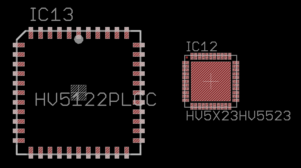
We all know the PLCC Style HV-Drivers from Microchip, for example HV5530.
All of them require a +12V Data Signal according to datasheet, but yet the run in some circuits with even 5V data signals..


While browsing microchips website i found HV5523/HV5623.
http://ww1.microchip.com/downloads/en/DeviceDoc/hv5523.pdf 

Those are fast 16Mhz registers with 5V logic data and can switch up to 220V@100mA per Channel and come in a very small QFN package. (Attached an image to PLCC for comparision)
I will definitly order some of them to test :) they would help to make a very slim and thin clock board :)


Has anyone experimented with them already? Something to know?


jb-electronics

unread,
Oct 28, 2017, 2:12:49 PM10/28/17
to neoni...@googlegroups.com
Sounds interesting! But I think the attached image didn't come through. Keep us posted! Jens
--
You received this message because you are subscribed to the Google Groups "neonixie-l" group.
To unsubscribe from this group and stop receiving emails from it, send an email to neonixie-l+...@googlegroups.com.
To post to this group, send email to neoni...@googlegroups.com.
To view this discussion on the web, visit https://groups.google.com/d/msgid/neonixie-l/103a52a5-137f-4708-9c7a-94b967d01421%40googlegroups.com.
For more options, visit https://groups.google.com/d/optout.


SWISSNIXIE - Jonathan F.

unread,
Oct 28, 2017, 2:24:13 PM10/28/17
to neonixie-l
Image  attached
ic.png

newxito

unread,
Oct 28, 2017, 2:29:32 PM10/28/17
to neonixie-l

Very interesting, thanks! I will order some of these chips but I think I will not be able to solder them correctly. There are some videos on youtube showing how to solder QFN packages using tons of flux and hot air...

gregebert

unread,
Oct 29, 2017, 12:13:48 AM10/29/17
to neonixie-l
I've used a heat gun to remove surface mount parts, but never to install one. I removed a device that looks like the aforementioned QFN, and the metal die-paddle on the bottom took a lot of heat to remove the part. I toasted the PCB because there was no heat-control; the PCB delaminated and had small bubbles but nothing actually 'burned'.

If you are going to assemble with these, use a reflow oven. I've seen several articles online about using a modified toaster oven. I only use SMT devices with visible pins or nubs, and only by hand-soldering.

Perhaps electrically-conductive epoxy could be used for die-paddle on the bottom of the device, and hand-soldering for everything else ?

Nick

unread,
Oct 29, 2017, 1:10:58 AM10/29/17
to neonixie-l
I was surprised that the data sheet didn't give more thermal information relating to the pad  - the chip, under load, dissipates up to 3.4W in a very small package, so the pad is important.

It'd have to be reflow for it to work - that along with appropriate board design to carry the heat away...

Nick

SWISSNIXIE - Jonathan F.

unread,
Oct 29, 2017, 4:03:35 AM10/29/17
to neonixie-l
Nick, note that the 3.4W are "absolute maximum" which usually means the part is going to die if you go over that.

The part it self needs only 5V@25mA (when switching) plus the losses of the hv switches.

In a nixie clock i guess there are always only 3 outputs on per chip.


I use the plcc 5122 which only has 1.2W heat dispatch and it doesnt get warm or so at all.

A crude way to solder the center pad is placing a hole under the chip and then solder it that way, but i'll give my planned board to a friend who has a soldering machine at work :)

Tomasz Kowalczyk

unread,
Oct 29, 2017, 5:56:20 AM10/29/17
to neonixie-l
I'm a bit concerned about spacing between pads. The device states it is able to switch voltages as high as 220V. The QFN package has spacing between the pads is nominally 0,25mm. This is violating norms about PCB spacing vs. voltage, the least strict norm I found states that 0,4mm spacing is required between traces with 220V between them - and that's for coated PCB, pads should have even higher spacing. Add to that the fact, that the IC will not be places 100% at the right spot, which will tighten pad-to-pad distance even more.

Of course, this should generally work, just like Chinese 230V/5V adapters, which often run secondary voltage traces very close to primary (and I haven't seen a single one which had the air gap actually cut - only marked). They do violate design rules, but at the same time, they do their job.

In nixie world enviroment all of this shouldn't matter - while a tube is connected just via the anode, it doesn't mean that cathodes are at anode potential. Cathodes are ~110V lower than anode potential, they will always represent a voltage drop of at least some value. That means that we can ignore some of the problems, because with a 180V supply, the Supertex piece will see only about 70V, which requires only 0,13mm spacing. Still, the uncoated spacing (pads) should be wider than this value.
I also do not know if leftover flux increases or decreases breakdown voltage of pad-to-pad spacing, and in such piece I highly believe that there will be a small space between PCB and IC, in which leftover flux will be gathering, and it will be not removable.

SWISSNIXIE - Jonathan F.

unread,
Oct 29, 2017, 8:37:24 AM10/29/17
to neonixie-l
My guess is that the usually known norms are only meant for AC Mains Voltage where you have to expect 220V RMS, meaning the peak is around 350V and you have to calculate with multiple kA short-circuit current in case of a short circuit.

Since Microchip clearly does not target hobby electronics, i guess they would'nt make a prodcuct that cant be uses when you want to comply with norms. Commercial brand producers have to comply with alot of tests and norms before they even can sell their end product.
These test would clearly fail if the space would be required to be 0.4mm and therefore they would never buy or consider using the HV5523 in the beginning if they would know that the IC would comply. I bet that there are alot of different norms for DC HV or "low current HV <500mA".

And another thing, i quess that the outputs are high-Z when they are off, and are connected to GND when they are on. So even if two pads would connect to each other, nothing spectacular or dangerous would happen. Even if a pad would connect to gnd, it would just result in a "always low" output.
Sinking 100mA per pin to ground by accident (usually the IC does the same by setting it HIGH) shouldt create any dangerous events like fire or so. Its much different than just conntect two AC (220V, 13Amps fused) Wires together with no load.

Since the "low voltage" pins have a single side for themselfs on the IC the risk of connecting HV to LV is much lower..


And yes, right, in a nixie enviroment it doesn't matter at all, usually a medium size tube consumes 2-4mA per tube

Paul Andrews

unread,
Oct 29, 2017, 9:52:53 AM10/29/17
to neonixie-l
I use the HV9808. 32 bits, hardware blanking, 5v control lines. Just set VPP to, say, 75V using a zener. Easy Peasy to program using an Arduino and the SPI library.

Nick

unread,
Oct 29, 2017, 10:05:03 AM10/29/17
to neoni...@googlegroups.com
On Sunday, 29 October 2017 12:03:35 UTC+4, SWISSNIXIE - Jonathan F. wrote:
Nick, note that the 3.4W are "absolute maximum" which usually means the part is going to die if you go over that.

I did note that - I state "up to 3.4W" - good engineering practice means you should still consider that...

Also, the PLCC package you use is about 300mm^2. at 1.2W, that's about 4mW/mm^2

The HV5523 QFN package is only 49mm^2, so at peak power that's 70mW/mm^2, i.e. nearly 18 times the power density of your chip.

Even if it was only 1.2W, that would still be 25mW/mm^2, i.e. 6 times the power density you are seeing with the HV5122.

The "plated-through hole underneath" technique works OK if done sensibly, but you still have to ensure that there is sufficient copper flooding to dissipate the heat.

Nick

EDITED: Changed the QFN size from 45 to 49mm^2


Tomasz Kowalczyk

unread,
Oct 29, 2017, 5:58:18 PM10/29/17
to neonixie-l
Having a thermal pad does wonders. A PLCC package, in socket or not, has to dissipate heat mainly through its body, because heat transfers to other parts of the board only via legs. In practice, almost all power is dissipated through plastic. Thermal pad allows to mostly transfer the heat to other metal bodies (copper area). However, the 3,4W is alot of heat and looking at conditions for such continous dissipation, the whole concept of a small PCB area is lost - 3x4" 4-layer board ( I assume that 3 layers are connected to the pad). In reality I doubt dissipating more than 1W on such piece would be allowable with thermal vias to other side and half a square inch of plane on the other side. However, judging from the datasheet, you can safely drive 3 CD-47 (with their 25mA cathode current) and still be way under 1W.

Back to the spacing topic: 
Mains voltage routing norms are way more strict than that. Mains isolation is calculated using alot higher voltage, I recall a number about 1200Vpp. 
Some norms I found require that the mains voltage should be at absolute minimum spaced 1,5mm from other traces and 2mm is recommended for basic design (and 4mm between primary and secondary). The norms I've taken for calculating minimum spacing were included in online clearance calculators and they assume the given voltage is peak AC or DC.
I really think that it would be unwise to use this chip to drive voltages close to 200V due to possiblity of arcing between pads. In nixie clock that would result in just two digits glowing at once, but that would still count as a failure. I'd like to see any report from testing this chip (pad width vs leaking current).

newxito

unread,
Nov 1, 2017, 10:08:17 AM11/1/17
to neonixie-l

I’ve got the HV5623 chips, really small stuff. Currently I’m designing a board, but I don’t have any experience with SMD components, so probably this will never work. Anyway, the plan is to feed the board with 5V over a micro-usb connector and to mount Yan’s new tiny PSU and a ESP32 on the board. Time to learn how to write apps. I’ll be back in 6 month. :-)

Paul Andrews

unread,
Dec 5, 2017, 4:06:25 PM12/5/17
to neonixie-l
I'm using one on a one-tube board I am making (a bit excessive for one tube, but it is small, 5V and can sink a decent current). At the moment I have one on a breadboard. They work as advertised! I picked up some Adafruit QFN44 adapters from digikey and had a stencil made to do the reflow with: I have hand soldered chips this small in the past, but it wasn't pretty and not always successful. A stencil makes it very easy.

I used a reflow griddle, which is fine for small stuff that I can pick up with kitchen implements.

I am thinking I will need to upgrade to an oven for the actual board though, which will have a bunch of QFN chips on it. Probably too big to pick up with the kitchen tools I have! That's why I am on this thread, I was looking for some info I saw pass by a while ago.

mchan

unread,
Feb 25, 2018, 4:26:41 PM2/25/18
to neonixie-l
This thread was from a few months ago but wanted to add something.  First those chips are pretty cool due to their size so i'll have to try soem at some point.

Secondly people keep saying the HV5530 needs 12V logic.  I've run these at 3.3V and all seems to be good.  I based this on the data sheet where it said Supply Voltage, VDD –0.5V to +15V

then Logic Input Levels –0.5V to VDD+0.5V

I interpreted that as plus or minus a half volt to the 3.3V it's running at.  Have I got that wrong and the fact it's "working" is a bit of a fluke ? :)


Tomasz Kowalczyk

unread,
Feb 25, 2018, 4:51:29 PM2/25/18
to neonixie-l
This was taken fron Absolute Maximum Ratings. There is a note right under them:
"Notice: Stresses above those listed under “Absolute Maximum Ratings” may cause permanent damage to the device. This is a stress rating only, and functional operation of the device at those or any other conditions above those indicated in the operational sections of this specification is not intended. Exposure to maximum rating conditions for extended periods may affect device reliability."

Right under that there are Recommended Operating Conditions, which clearly state VDD 10,2-13,8V and logic input between VDD-2V to VDD. So if it works at 3,3V logic, then good for you, but if something unexpected happens, then manufacturer takes no responsibility, as you use it out of Recommended Operating Conditions.

Shortly speaking, area between ROC and AMR is treated like "it won't burn, but it doesn't have to work". AMR is the limit of permanent damage of the chip, while ROC determines range in which manufacturer guarantees, that information found in the datasheet will be accurate.

So it is up to you. If the clock is running at your home, then an unexpected failure won't be a disaster. But I would never sell a clock with parts operating out of specifications.

mchan

unread,
Feb 25, 2018, 5:27:41 PM2/25/18
to neonixie-l
yes i saw the ROC. my main reason for loosely interpreting the max ratings and going with something within that range was to reduce components (for level shifting and what not).  I imagine the better way for me to interpret is to think that the closer I get to the MAX ratings the more likely it could fail.
I think for my next clock with these chips I'll get closer to ROC and do things "right".  but for now i'm a few volts within the MAX ratings so hopefully all is good and things continue working OK.  This is, as you mentioned, for home use so I don't have to worry too much if it fails.

this clock in question is here


I do have room for the additional components to get things to ROC but didn't at the time think it necessary.   However theres always NEXT TIME ! :)

thanks for the info... very helpful!

Dekatron42

unread,
Feb 26, 2018, 2:51:50 PM2/26/18
to neonixie-l
Have you asked Microchip what they think about the use? They have always been very helpful when I have asked them about their ic's and the ratings.

/Martin
Reply all
Reply to author
Forward
0 new messages