More higher layer support

Liang Jia

Stefan Weber
Liang Jia

Wayne Stambaugh
Hi Liang,
The LSET object is merely where it's possible to add new layers
but doing so will not be helpful and possibly harmful if you don't
understand how layers work internally. Virtually every object on
boards and footprints has to understand what the layers mean in
order for them to work properly and the tools used to create and
edit them. This doesn't include all of the DRC and UI changes
that would have to be updated for the layer changes. I don't see
this feature request being done by anyone without years of
experience with the KiCad code base. It is a major undertaking.
It's on the development team's list of new features but it's not
one that is requested very often (there are just not that many
users that require more than 32 copper layers) so it may not make
it into version 8.
Cheers,
Wayne
--
You received this message because you are subscribed to the Google Groups "KiCad Developers" group.
To unsubscribe from this group and stop receiving emails from it, send an email to devlist+u...@kicad.org.
To view this discussion on the web visit https://groups.google.com/a/kicad.org/d/msgid/devlist/CAE0Ak8aJeP3F%2BbPgkJveQR_BThu2F%3D-T9kh63UnLBi5fti7DxQ%40mail.gmail.com.
Liang Jia
To view this discussion on the web visit https://groups.google.com/a/kicad.org/d/msgid/devlist/42d3e1b6-4fa2-b04e-4dc2-c11bfa9844dd%40gmail.com.
Wayne Stambaugh
Hi Liang,
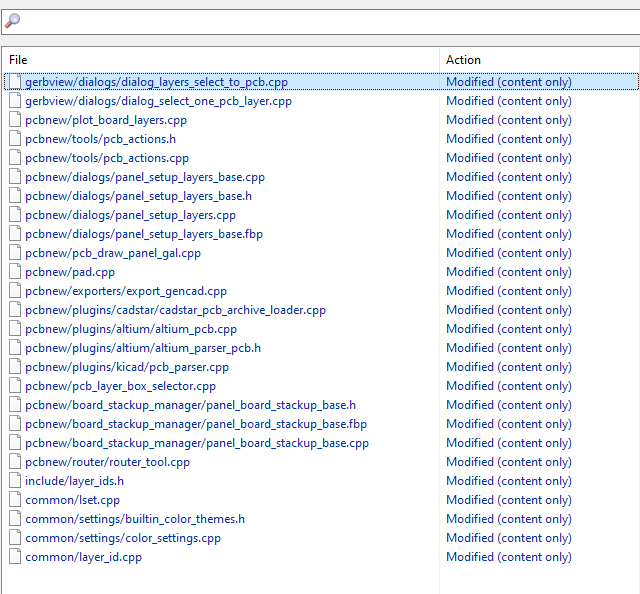
I would be surprised if the this was all the files that needed to be updated in order to add more copper layers. Without actually seeing your changes, it's impossible for me to know for sure. I don't see any DRC source file changes and it appears that you didn't change the file version both of which seem to point to an incomplete implementation. Also, if you are going to maintain your own fork of KiCad, please change the "generator" token in the board file format to something other than "pcbnew". This way if someone attempts to file a bug against your changes, we will immediately know that the files did not come from KiCad.
I'm curious what your trying to accomplish here. If you are intending to merge your changes back into KiCad, you need to be working closely with the KiCad lead development team. Making large change sets to KiCad without coordinating with the KiCad lead developers rarely leads to the outcome that new developers expect. One thing I should caution you on is that the lead development team is planning on allowing any number of copper or user layers instead of just increasing the current count of those layers. This is fundamentally a much larger project because it will require significant internal changes virtually all of the PCB code.
If you are interested in contributing to the KiCad project, I
recommend that you take a look at the Contributing to
KICad web page.
Cheers,
Wayne
To view this discussion on the web visit https://groups.google.com/a/kicad.org/d/msgid/devlist/CAE0Ak8b_kU0E%2BJTaW_kfxiqx08xH9k5Me9DTc8pr91OjQNynrw%40mail.gmail.com.
Liang Jia
To view this discussion on the web visit https://groups.google.com/a/kicad.org/d/msgid/devlist/fb79406b-ccf9-f776-9a2e-e0397d66e7e9%40gmail.com.
Wayne Stambaugh
Hi Liang,
I don't have time right now to look over your patch given it's
size. It's far easier to other developers to review changes using
GitLab's interface rather than applying your patch directly (which
may not apply cleanly given the changes in both the master and 7.0
branches) and reviewing them. You should push your 64 layer
branch to your private GitLab repo and publish the link to it so
other developers can pull from that branch to review and test your
changes. It will also make your life easier if at some point in
the future you choose to submit a merge request to the KiCad
project.
The board file version definitions are kept in
https://gitlab.com/kicad/code/kicad/-/blob/master/pcbnew/plugins/kicad/pcb_plugin.h
They are defined as the date the file format changed using the
YYYYMMDD format.
The board file plugin header formatting for changing the generator name is here https://gitlab.com/kicad/code/kicad/-/blob/master/pcbnew/plugins/kicad/pcb_plugin.cpp#L300
I hope this helps.
Wayne
To view this discussion on the web visit https://groups.google.com/a/kicad.org/d/msgid/devlist/CAE0Ak8ZRO%2BWbo-UXh9K%2BdU6bPX6jnkzGgA2WR1YXHe2r5Ari2w%40mail.gmail.com.
Liang Jia
To view this discussion on the web visit https://groups.google.com/a/kicad.org/d/msgid/devlist/357a9de5-f1f3-a178-b573-8409c151c4cb%40gmail.com.