PandaBoard WLAN Antenna

John (USP)
strange to me. If you look at reference layout for chip antennas from most
suppliers, they have a ground plane with a 50 Ohm RF feed line to one side
of the chip antenna. The other side of the chip antenna is left floating and
clear of any ground plane. General rule dictates that the ground plane is at
least 2mm clear of the antenna.
Here is a good example of recommended PCB layout for chip antenna.
http://www.johansontechnology.com/en/technical-notes/integrated-passives-rf-
comp/chip-antenna-layout-considerations-for-80211.html
The PandaBoard antenna is surrounded by ground plane so I'm not sure how
this antenna is able to radiate. Would it be possible for the antenna
designer to write a brief explanation of how or why this antenna design
works?
Regards,
John

nip...@hotmail.com
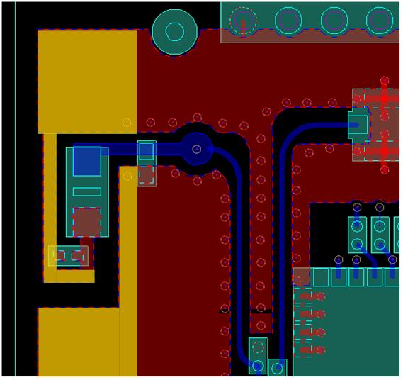
Sorry I'm not the designer, but we have verified BT/WLAN on panda but maybe there could be performance issues due to what you're highlighting below?
From the site you referred to are you recommending removing the ground in the areas highlighted in yellow in the attached image?
Also, can you please suggest this and/or any other changes you can think of here so that we can consider them for a future re-spin of the board?
http://omappedia.org/wiki/PandaBoard_Errata
Best Regards -Nipuna
----------------------------------------
> From: jsyn...@us-power.com
> To: panda...@googlegroups.com
> Subject: [pandaboard] PandaBoard WLAN Antenna
> Date: Wed, 13 Oct 2010 22:04:33 -0700

John (GMail)
> -----Original Message-----
> From: panda...@googlegroups.com [mailto:panda...@googlegroups.com]
> On Behalf Of nip...@hotmail.com
> Sent: Friday, October 15, 2010 1:44 PM
> To: Nipuna Gunasekera
> Subject: RE: [pandaboard] PandaBoard WLAN Antenna
>
>
> Sorry I'm not the designer, but we have verified BT/WLAN on panda but
maybe
> there could be performance issues due to what you're highlighting below?
> From the site you referred to are you recommending removing the ground in
the
> areas highlighted in yellow in the attached image?
I only used that document as an example, but you can review layout
suggestions from several chip antenna suppliers and they all look similar to
the document I referenced. I suggest you contact an antenna design
specialist with the required expertise. I have copied this e-mail to Tim
Milam from Custom Integrated Antennas whom we have used in the past. Tim has
probably designed most of the antennas used in Bluetooth devices available
today. Tim can evaluate the performance of your existing antenna design
which might be helpful in deciding how you move forward.
Regards,
John
>
> Also, can you please suggest this and/or any other changes you can think
of here so
> that we can consider them for a future re-spin of the board?
> http://omappedia.org/wiki/PandaBoard_Errata
>
> Best Regards -Nipuna
>
>
> ----------------------------------------
> > From: jsyn...@us-power.com
> > To: panda...@googlegroups.com
> > Subject: [pandaboard] PandaBoard WLAN Antenna
> > Date: Wed, 13 Oct 2010 22:04:33 -0700
> >
> > I was looking at the PandaBoard PCB layout and the WLAN antenna design
> > looks strange to me. If you look at reference layout for chip antennas
> > from most suppliers, they have a ground plane with a 50 Ohm RF feed
> > line to one side of the chip antenna. The other side of the chip
> > antenna is left floating and clear of any ground plane. General rule
> > dictates that the ground plane is at least 2mm clear of the antenna.
> >
> > Here is a good example of recommended PCB layout for chip antenna.
> >
> > http://www.johansontechnology.com/en/technical-notes/integrated-passiv
> > es-rf- comp/chip-antenna-layout-considerations-for-80211.html

Timothy Milam
I followed the link below and the only file I saw was the jpg of the area
closely surrounding the antenna. The jpg didn't have good enough detail to
see if all of the metalization surrounding the chip was actually ground or
not. If it is there may be concern, but a determination of that would also
depend on the application of the target product.
One thought I had, based on the low resolution image was that one side of
the metalization might not be attached to PCB's ground system and therefore
may be serving as a parasitic element for the antenna to enhance or redirect
the pattern.
With no more detailed information the low resolution jpg, that is about all
the comment I can offer at this time, other than you were correct that most
of these chip antennas do need to be separated from the ground plane --> so
they can behave as resonant elements for monopole/dipole antenna structures.
Good catch, if this is early in the design cycle it could save a lot of
money and schedule delay in the long run.
Thank You,
Tim
Proprietary Information Clause:
This electronic mail (e-mail) transmission is private and intended solely
for the individual (s), entity, or entities that are the intended recipients
and with a need to possess this information. The text of this e-mail and
(or) any attachments thereof may contain information that is restricted,
sensitive, privileged, proprietary, competitive, and/or confidential to the
sender and to some or all parties to which it is addressed. If you have
received this transmission in error, you are not authorized to read, copy,
print, retain, disclose, disseminate, distribute, or use this message its
attachments or any part thereof and any one of these acts may be in
violation of local, state, and (or) federal law. Please transmit a reply
message informing the sender that it was misdirected, then delete the
original e-mail, any attachment (s), and the reply and all copies thereof
(including backup copies) that have been made of the original e-mail, any
attachments, and the reply. Thank you for your kind consideration in this
matter.
Timothy Milam
Custom Integrated Antennas
2715 KY Hyw 610 W, PO Box 126
Virgie, KY 41572
Tel: (512) 638-2643
Fax: (512) 532-0947