Jaluino intermediate shield (aka "Styx") to plug Arduino shields
10 views
Skip to first unread message

Sebastien Lelong
Sep 10, 2009, 12:23:34 PM9/10/09
to jal...@googlegroups.com
Hi guys,
I've committed Jaluino PCB & schematic template for Eagle (see http://code.google.com/p/jallib/source/browse/trunk/project/jaluino/schematics/jaluino_shield_template_eagle.zip). From this, I tried to create a shield that could act as a layer, an intermediate, between Jaluino shields and Arduino shields. The idea is to plug this intermediate shield onto Jaluino board, then plug an original Arduino shield on top of this.
Attached are pictures of:
- schematic: with mapping between Jaluino & Arduino pins. For PWM channels, one is taken from RC2/CCP1, another is taken either from RC1/CCP2 or RB3/CCP2. RC1 and RB3 are multiplexed, so you can choose which of these two pins will carry PWM. Using this approach, it may increase compatibility (still only 2 PWM channels will be available, but for one, you can choose where). As for analog pins, RA3/AN3 is mapped with AREF. Other mappings are quite explicit. I'm open to suggestions !
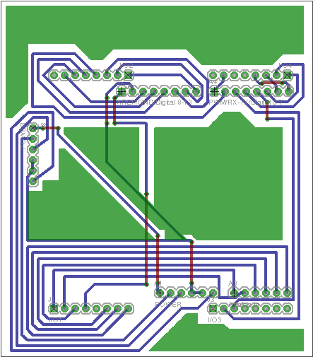
- PCB: the resulting PCB. Green aeras are considered as blue tracks (but couldn't make them blue...). Quite a lot of vias, not that beautiful, sorry...
Finally, I had a hard brainstorming (not just with myself this time), to find a name for this shield: "Styx". So this is Jaluino "Styx" shield. Why ? Well... Well in Greek Mythology, Styx is the river between Earth and Underworld, a clear frontier between two worlds. I hope this illustrates as good as possible the main purpose of this shield. Defining which part is Earth, which part is Underworld in our case is left to readers' objectivity :)
http://en.wikipedia.org/wiki/Styx for more...

Cheers,
Seb
--
Sébastien Lelong
http://www.sirloon.net
http://sirbot.org
I've committed Jaluino PCB & schematic template for Eagle (see http://code.google.com/p/jallib/source/browse/trunk/project/jaluino/schematics/jaluino_shield_template_eagle.zip). From this, I tried to create a shield that could act as a layer, an intermediate, between Jaluino shields and Arduino shields. The idea is to plug this intermediate shield onto Jaluino board, then plug an original Arduino shield on top of this.
Attached are pictures of:
- schematic: with mapping between Jaluino & Arduino pins. For PWM channels, one is taken from RC2/CCP1, another is taken either from RC1/CCP2 or RB3/CCP2. RC1 and RB3 are multiplexed, so you can choose which of these two pins will carry PWM. Using this approach, it may increase compatibility (still only 2 PWM channels will be available, but for one, you can choose where). As for analog pins, RA3/AN3 is mapped with AREF. Other mappings are quite explicit. I'm open to suggestions !
- PCB: the resulting PCB. Green aeras are considered as blue tracks (but couldn't make them blue...). Quite a lot of vias, not that beautiful, sorry...
Finally, I had a hard brainstorming (not just with myself this time), to find a name for this shield: "Styx". So this is Jaluino "Styx" shield. Why ? Well... Well in Greek Mythology, Styx is the river between Earth and Underworld, a clear frontier between two worlds. I hope this illustrates as good as possible the main purpose of this shield. Defining which part is Earth, which part is Underworld in our case is left to readers' objectivity :)
http://en.wikipedia.org/wiki/Styx for more...
Cheers,
Seb
--
Sébastien Lelong
http://www.sirloon.net
http://sirbot.org

vasile surducan
Sep 10, 2009, 1:26:59 PM9/10/09
to jal...@googlegroups.com
Hi Seb,
I am appreciating your enthusiasm, however the shield you've designed it hasn't too much ability of shielding.
If your need carrying PWM signals from one board to other, where both or only one board has also analogic areas, you must be very carefull. You need two layers and ground planes on both layers connected through a number of vias.
If your application is pure digital, both boards without any analogic area, then shielding is not important.
If the PWM is used for generating a clean analogic signal after a filter, could be a serious problem (clean PWM filtering with first order filters is impossible, no matter what you have seen on the enthusiastics websites; clean means lower than 5mV ripple).
Learn to avoid in your design 90 degree direction changes in your routes as a general rule. If you have two layers, use traces equaly on both layers. Avoid multiple layer changes on clocks, PWMs and other agressing signals. Designing a PCB it's like programming. You can't do it well if you don't do it continously...Biggest problems start on 8-12 layers, but two layers an a PIC it's a good start.
Sebastien Lelong
Sep 10, 2009, 1:47:03 PM9/10/09
to jal...@googlegroups.com
Hi Vasile,
Thanks for your feeback. Indeed, this is a naive PCB I have here, but I'm afraid I can't do more by myself...
"shield", is the sense of a "physical" shield over the main board.
Original Arduino's shields have 2 GND pins, as for here. I can't build real two layers PCB at home. Red lines are for bridges (or vias).
OK
Yeah you're right. I'm not continuously building PCB, but I'm continuously trying to sometime build some :) I'm very respectful for people who knows how to do this, like Richard. His Jaluino design is very clean, yet very easy to build.
I'll think more about this, and may provide another PCB for this "Styx" shield. The problem is despite the fact there aren't many components, you have to map pins so lots of cross. I may also re-map pins to a more natural layout.
Thanks.
Seb
Thanks for your feeback. Indeed, this is a naive PCB I have here, but I'm afraid I can't do more by myself...
I am appreciating your enthusiasm, however the shield you've designed it hasn't too much ability of shielding.
"shield", is the sense of a "physical" shield over the main board.
If your need carrying PWM signals from one board to other, where both or only one board has also analogic areas, you must be very carefull. You need two layers and ground planes on both layers connected through a number of vias.
Original Arduino's shields have 2 GND pins, as for here. I can't build real two layers PCB at home. Red lines are for bridges (or vias).
If your application is pure digital, both boards without any analogic area, then shielding is not important.
OK
If the PWM is used for generating a clean analogic signal after a filter, could be a serious problem (clean PWM filtering with first order filters is impossible, no matter what you have seen on the enthusiastics websites; clean means lower than 5mV ripple).Learn to avoid in your design 90 degree direction changes in your routes as a general rule. If you have two layers, use traces equaly on both layers. Avoid multiple layer changes on clocks, PWMs and other agressing signals. Designing a PCB it's like programming. You can't do it well if you don't do it continously...Biggest problems start on 8-12 layers, but two layers an a PIC it's a good start.
Yeah you're right. I'm not continuously building PCB, but I'm continuously trying to sometime build some :) I'm very respectful for people who knows how to do this, like Richard. His Jaluino design is very clean, yet very easy to build.
I'll think more about this, and may provide another PCB for this "Styx" shield. The problem is despite the fact there aren't many components, you have to map pins so lots of cross. I may also re-map pins to a more natural layout.
Thanks.
Seb
On 9/10/09, Sebastien Lelong <sebastie...@gmail.com> wrote:
Hi guys,
I've committed Jaluino PCB & schematic template for Eagle (see http://code.google.com/p/jallib/source/browse/trunk/project/jaluino/schematics/jaluino_shield_template_eagle.zip). From this, I tried to create a shield that could act as a layer, an intermediate, between Jaluino shields and Arduino shields. The idea is to plug this intermediate shield onto Jaluino board, then plug an original Arduino shield on top of this.
Attached are pictures of:
- schematic: with mapping between Jaluino & Arduino pins. For PWM channels, one is taken from RC2/CCP1, another is taken either from RC1/CCP2 or RB3/CCP2. RC1 and RB3 are multiplexed, so you can choose which of these two pins will carry PWM. Using this approach, it may increase compatibility (still only 2 PWM channels will be available, but for one, you can choose where). As for analog pins, RA3/AN3 is mapped with AREF. Other mappings are quite explicit. I'm open to suggestions !
- PCB: the resulting PCB. Green aeras are considered as blue tracks (but couldn't make them blue...). Quite a lot of vias, not that beautiful, sorry...
Finally, I had a hard brainstorming (not just with myself this time), to find a name for this shield: "Styx". So this is Jaluino "Styx" shield. Why ? Well... Well in Greek Mythology, Styx is the river between Earth and Underworld, a clear frontier between two worlds. I hope this illustrates as good as possible the main purpose of this shield. Defining which part is Earth, which part is Underworld in our case is left to readers' objectivity :)
http://en.wikipedia.org/wiki/Styx for more...
Sebastien Lelong
Sep 10, 2009, 2:39:38 PM9/10/09
to jal...@googlegroups.com
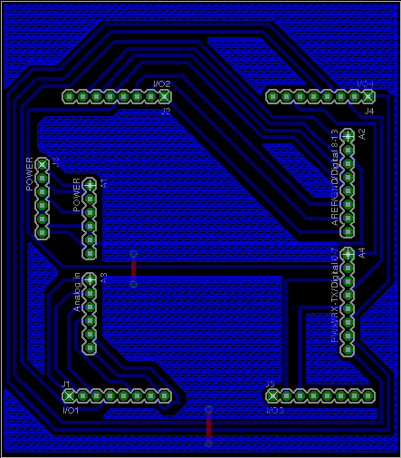
This one might be better, there's no bridge except two for connecting large areas of GND signals (I don't know if this is much useful...)
2009/9/10 vasile surducan <vsur...@gmail.com>

funlw65
Sep 10, 2009, 3:13:05 PM9/10/09
to jallib
I like this one!
Vasi
On Sep 10, 9:39 pm, Sebastien Lelong <sebastien.lel...@gmail.com>
wrote:
> 28KViewDownload
Vasi
On Sep 10, 9:39 pm, Sebastien Lelong <sebastien.lel...@gmail.com>
wrote:
> This one might be better, there's no bridge except two for connecting large
> areas of GND signals (I don't know if this is much useful...)
>
> Seb
> --
> Sébastien Lelonghttp://www.sirloon.nethttp://sirbot.org
>
> 2009/9/10 vasile surducan <vsurdu...@gmail.com>
> areas of GND signals (I don't know if this is much useful...)
>
> Seb
> --
> Sébastien Lelonghttp://www.sirloon.nethttp://sirbot.org
>
>
> > Hi Seb,
>
> > I am appreciating your enthusiasm, however the shield you've designed it
> > hasn't too much ability of shielding.
>
> > If your need carrying PWM signals from one board to other, where both or
> > only one board has also analogic areas, you must be very carefull. You need
> > two layers and ground planes on both layers connected through a number of
> > vias.
>
> > If your application is pure digital, both boards without any analogic area,
> > then shielding is not important.
>
> > If the PWM is used for generating a clean analogic signal after a
> > filter, could be a serious problem (clean PWM filtering with first order
> > filters is impossible, no matter what you have seen on the enthusiastics
> > websites; clean means lower than 5mV ripple).
>
> > Learn to avoid in your design 90 degree direction changes in your routes as
> > a general rule. If you have two layers, use traces equaly on both
> > layers. Avoid multiple layer changes on clocks, PWMs and other agressing
> > signals. Designing a PCB it's like programming. You can't do it well if you
> > don't do it continously...Biggest problems start on 8-12 layers, but two
> > layers an a PIC it's a good start.
>
> > On 9/10/09, Sebastien Lelong <sebastien.lel...@gmail.com> wrote:
>
> >> Hi guys,
>
> >> I've committed Jaluino PCB & schematic template for Eagle (see
> >>http://code.google.com/p/jallib/source/browse/trunk/project/jaluino/s...).
>
> >> Hi guys,
>
> >> I've committed Jaluino PCB & schematic template for Eagle (see
> >> From this, I tried to create a shield that could act as a layer, an
> >> intermediate, between Jaluino shields and Arduino shields. The idea is to
> >> plug this intermediate shield onto Jaluino board, then plug an original
> >> Arduino shield on top of this.
>
> >> Attached are pictures of:
>
> >> - schematic: with mapping between Jaluino & Arduino pins. For PWM
> >> channels, one is taken from RC2/CCP1, another is taken either from RC1/CCP2
> >> or RB3/CCP2. RC1 and RB3 are multiplexed, so you can choose which of these
> >> two pins will carry PWM. Using this approach, it may increase compatibility
> >> (still only 2 PWM channels will be available, but for one, you can choose
> >> where). As for analog pins, RA3/AN3 is mapped with AREF. Other mappings are
> >> quite explicit. I'm open to suggestions !
>
> >> - PCB: the resulting PCB. Green aeras are considered as blue tracks (but
> >> couldn't make them blue...). Quite a lot of vias, not that beautiful,
> >> sorry...
>
> >> Finally, I had a hard brainstorming (not just with myself this time), to
> >> find a name for this shield: "Styx". So this is Jaluino "Styx" shield. Why ?
> >> Well... Well in Greek Mythology, Styx is the river between Earth and
> >> Underworld, a clear frontier between two worlds. I hope this illustrates as
> >> good as possible the main purpose of this shield. Defining which part is
> >> Earth, which part is Underworld in our case is left to readers' objectivity
> >> :)
>
> >>http://en.wikipedia.org/wiki/Styxfor more...
> >> intermediate, between Jaluino shields and Arduino shields. The idea is to
> >> plug this intermediate shield onto Jaluino board, then plug an original
> >> Arduino shield on top of this.
>
> >> Attached are pictures of:
>
> >> - schematic: with mapping between Jaluino & Arduino pins. For PWM
> >> channels, one is taken from RC2/CCP1, another is taken either from RC1/CCP2
> >> or RB3/CCP2. RC1 and RB3 are multiplexed, so you can choose which of these
> >> two pins will carry PWM. Using this approach, it may increase compatibility
> >> (still only 2 PWM channels will be available, but for one, you can choose
> >> where). As for analog pins, RA3/AN3 is mapped with AREF. Other mappings are
> >> quite explicit. I'm open to suggestions !
>
> >> - PCB: the resulting PCB. Green aeras are considered as blue tracks (but
> >> couldn't make them blue...). Quite a lot of vias, not that beautiful,
> >> sorry...
>
> >> Finally, I had a hard brainstorming (not just with myself this time), to
> >> find a name for this shield: "Styx". So this is Jaluino "Styx" shield. Why ?
> >> Well... Well in Greek Mythology, Styx is the river between Earth and
> >> Underworld, a clear frontier between two worlds. I hope this illustrates as
> >> good as possible the main purpose of this shield. Defining which part is
> >> Earth, which part is Underworld in our case is left to readers' objectivity
> >> :)
>
>
> >> [image: Dor%C3%A9_-_Styx.jpg]
>
> >> Cheers,
> >> Seb
> >> --
> >> Sébastien Lelong
> >>http://www.sirloon.net
> >>http://sirbot.org
>
>
>
> jaluino_shield_styx_pcb.png
> >> [image: Dor%C3%A9_-_Styx.jpg]
>
> >> Cheers,
> >> Seb
> >> --
> >> Sébastien Lelong
> >>http://www.sirloon.net
> >>http://sirbot.org
>
>
>
> 28KViewDownload
vasile surducan
Sep 11, 2009, 3:01:42 AM9/11/09
to jal...@googlegroups.com
Hi Seb,
Unconected shield areas acts as antennas for the adjacent signals near the area.
I think the GND should be also connected to some connectos.
For a goos shield design at home, use a double layer PCB, design routes on one layer and keep the other layer as ground isolating the component pins with a large drill in the copper (ie, a 0.8 drill diameter, 1.5 or 2mm diameter for copper isolation). This tehnique is used to produce high quality RF PCB's at home.
Connect with more vias (at least 10-20 for DC or PICmicro design and up to thousens for RF - not suitable for home) between the ground planes of the layers.
Try to go smaller as possible with your PCB designs, keeping an easy way to replace any components. This is the right way for increasing PCB design performance.
Sebastien Lelong
Sep 11, 2009, 8:45:53 AM9/11/09
to jal...@googlegroups.com
Hi Vasile,
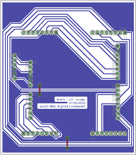
I've committed my last try, including aeras with GND signals, propagated over the board (I've finally managed to use polygons with rastness option).
GND is currently connected to 3 pins, 2 pins adjacent, and 1 on another connector. I can't decide where to put GND on pins, this is imposed by either Jaluino pins or Arduino pins.
I've committed my last try, including aeras with GND signals, propagated over the board (I've finally managed to use polygons with rastness option).
Unconected shield areas acts as antennas for the adjacent signals near the area.I think the GND should be also connected to some connectos.
GND is currently connected to 3 pins, 2 pins adjacent, and 1 on another connector. I can't decide where to put GND on pins, this is imposed by either Jaluino pins or Arduino pins.
For a goos shield design at home, use a double layer PCB, design routes on one layer and keep the other layer as ground isolating the component pins with a large drill in the copper (ie, a 0.8 drill diameter, 1.5 or 2mm diameter for copper isolation). This tehnique is used to produce high quality RF PCB's at home.
Connect with more vias (at least 10-20 for DC or PICmicro design and up to thousens for RF - not suitable for home) between the ground planes of the layers.Try to go smaller as possible with your PCB designs, keeping an easy way to replace any components. This is the right way for increasing PCB design performance.
I can't produce a double layer PCB at home... More, as I said, these shields aren't RF shields, but "just" daughter boards. In any case, I clearly won't fell confortable when it come the time to design advanced high quality RF PCBs... :)
I'll try to build the current one, as a Proof Of Concept. It'll mainly be used to plug prototype board, like this one: http://www.ladyada.net/images/pshield/miniproto.jpg . As for other more advanced Arduino shield, we'll have to check... or design our own.
I'll try to build the current one, as a Proof Of Concept. It'll mainly be used to plug prototype board, like this one: http://www.ladyada.net/images/pshield/miniproto.jpg . As for other more advanced Arduino shield, we'll have to check... or design our own.

Richard
Sep 11, 2009, 3:15:40 PM9/11/09
to jallib
Hoi Seb,
Very nice board, but I think it’s better to make the lines as short as
possible instead of trying to create as much ground planes as
possible,
You don’t need the via, create without via’s as big as possible ground
plane.
This is more for keeping your ets flowed longer good than it is for
avoiding interference between wires.
You also don’t need to connect ground to extra pins, don’t make it
unnecessary complex.
It was smart to turn your arduino connectors and thereby lose the
via’s :-)
Greetz
Richard
Sebastien Lelong
Sep 12, 2009, 4:19:57 AM9/12/09
to jal...@googlegroups.com
Hi Richard,
OK. I placed headers, and clicked autorouting, resulting in this... :)
OK, I already printed the PCB, but I won't connect vias.
Simplified a lot the PCB...
As I said, I've already printed the PCB (and won't access laser printer for days), and may build Styx shield this WE. Clearly this is not the perfect shield, but more like a Proof Of Concept / POC (and also take photos of Jaluino with a shield :)). If it reveals interesting, we may improve the design as needed.
Cheers,
Seb
--
Sébastien Lelong
Very nice board, but I think it’s better to make the lines as short as
possible instead of trying to create as much ground planes as
possible,
OK. I placed headers, and clicked autorouting, resulting in this... :)
You don’t need the via, create without via’s as big as possible ground
plane.
OK, I already printed the PCB, but I won't connect vias.
This is more for keeping your ets flowed longer good than it is for
avoiding interference between wires.
You also don’t need to connect ground to extra pins, don’t make it
unnecessary complex.
It was smart to turn your arduino connectors and thereby lose the
via’s :-)
Simplified a lot the PCB...
As I said, I've already printed the PCB (and won't access laser printer for days), and may build Styx shield this WE. Clearly this is not the perfect shield, but more like a Proof Of Concept / POC (and also take photos of Jaluino with a shield :)). If it reveals interesting, we may improve the design as needed.
Cheers,
Seb
--
Sébastien Lelong
Sebastien Lelong
Sep 13, 2009, 9:33:02 AM9/13/09
to jal...@googlegroups.com
Errrr...... I printed it the wrong way (upside down), one connector is on the wrong place. I can't build this shield right now... :[
2009/9/12 Sebastien Lelong <sebastie...@gmail.com>
Reply all
Reply to author
Forward
0 new messages